


Your Trusted Prototype PCB Manufacturing And Assembly Partner.
When you partner with us, we do everything to ensure your PCB manufacturing and assembly are completed on time to your specifications with the highest quality.
Leading manufacturer of PCB Fabrication and Assembly in China.
PCB via holes are crucial components of any printed circuit board. They serve as an essential link between different layers of a PCB, allowing for the transfer of electrical signals between the layers. The size, plugging, and filling of via holes play an important role in determining the overall performance and reliability of a PCB, while tolerance is a critical factor in ensuring that the PCB meets the necessary specifications. There are several types of via holes, including blind vias, buried vias, and through vias, each with their unique characteristics and applications. Thermal considerations are also crucial for via design, particularly for high-power and high-speed applications. In this comprehensive guide, we will explore everything you need to know about PCB via holes, including their types, design, manufacturing, testing, applications, and future trends.
A via hole is an essential component of a printed circuit board that provides a conductive path between the different layers of the board. It is a small hole that is drilled through the board and plated with metal to form a connection between the copper traces on different layers. Via holes are used to connect the different layers of copper traces that make up the conductive paths on a PCB, allowing signals and power to be transmitted between components and traces on different layers. Via holes come in different sizes, types, and shapes, and their design and placement can have a significant impact on the performance and reliability of the PCB.
A via consists of:
PCB via holes serve as vertical conduits that connect different layers of a PCB. Here are some of their main functions:
Enabling electrical connections: Via holes are vital in connecting components and traces on different layers of a PCB.
Miniaturization: Via holes allow the manufacture of compact PCBs with a high component density, which is important in designs where size is a critical factor.
Noise reduction: When a PCB has several components, there’s a chance that electrical noise can be generated on the surface of the board. Via holes ground the board and minimize the amount of noise present.
Efficient use of PCB space: Via holes enable routing of traces on different layers of the board, thereby ensuring that the available PCB real estate is used efficiently.
Signal integrity: Via holes help to maintain signal integrity by ensuring that the impedance levels remain consistent across the PCB.
Thermal management: Via holes play a critical role in dissipating heat generated by electronic components, particularly when designing power electronics.
In conclusion, the importance of PCB via holes in modern electronics designs cannot be overstated. They are essential in enabling electrical connections, minimizing noise, efficient use of PCB space, and ensuring signal integrity and thermal management.
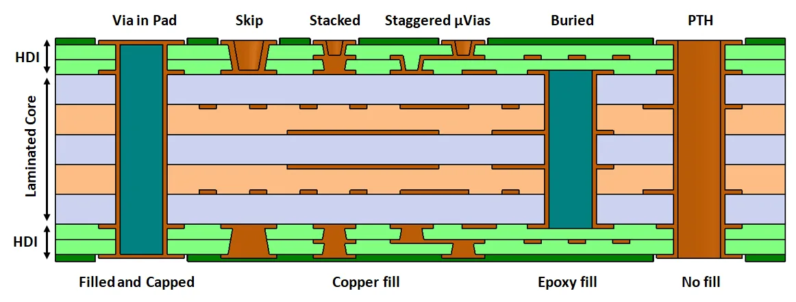
There are several types of PCB via holes, including through-hole, blind via, buried via and micro via.
Through-hole via: This type of via goes all the way through the PCB from the top surface to the bottom surface and is used for connecting circuits on different layers.
Blind via: This type of via connects the outermost layer of the PCB to one or more inner layers, but does not extend through the entire board.
Buried via: This type of via connects one or more inner layers of the PCB, but does not extend to the outermost layer.
Micro via: This type of via is typically less than 0.15mm in diameter and is used in high-density circuit boards where there is limited space for the via. Micro via technology enables the routing of traces between small components.
Via in Pad: Via in pad is a type of through-hole via that is used in PCB design. It involves routing a via hole directly beneath a pad on the PCB, so that the via and the pad share the same physical space. This technique can be especially useful for creating high-density PCBs where space is at a premium. Via in pad technology can help maximize the available PCB space while reducing the number of layers needed for interconnections. It also enables better thermal management and can improve signal integrity. However, the use of via in pad can also present some challenges during manufacturing, assembly, and testing, so it’s important to carefully consider the trade-offs before using this technology in a given design.
PCB via holes are an essential part of printed circuit board designs. They allow for electrical connections between different layers of the board and promote miniaturization, noise reduction, and temperature control. To give a better understanding of the different types of via holes that can be used in PCB designs, we can classify them based on their usage and shape. Based on their usage, via holes can be classified into signal via, power via, ground via, and stacked via. On the other hand, via holes can also be classified based on their shape which includes round via, square via, oblong via, and tear-shaped via. Each of these classifications has its unique characteristics and properties that make them suitable for use in specific PCB designs. Let’s take a closer look at both classifications and their applications in PCB design.
A. Classification Based on Usage
Via holes can be classified into several categories based on their usage, such as:
B. Classification Based on Shape
Via holes can also be classified based on their shape, such as:
There are a few steps involved in the process of making PCB vias. First, drill holes are made on the board where the vias will be placed. These holes are typically made using a CNC drilling machine with appropriately sized drill bits based on the desired via size. The conventional PCB manufacturing process only permits through-hole configurations. However, depth-controlled drilling techniques, such as laser drilling, can offer a wider range of via options.
After the holes are drilled, the board is cleaned and prepared for via filling. There are two main filling methods: PSR Via Fill and RESIN Via Fill. PSR Via Fill involves filling the via holes with a conductive paste such as solder paste. RESIN Via Fill involves filling the via holes with a non-conductive material such as epoxy resin.
Once the vias are filled using the desired method, excess filling material is removed using a process such as planarization or laser ablation. This ensures that the vias are smoothed out and the board surface is level.
Finally, the board is cleaned again and any necessary finishing processes are applied such as HASL or ENIG plating.
It’s important to note that different via sizes may require different filling methods and materials. For example, smaller via holes may need to be filled with solder paste while larger via holes may require epoxy resin. Additionally, the filling material used can vary based on requirements such as heat dissipation, conductivity, or insulation.
When it comes to PCBs, via holes play an important role in the electrical connection between different layers. Via holes are drilled holes that connect two or more layers of the PCB with a copper barrel. Via hole size is one of the critical factors that can affect the performance of the PCB.
The size of via holes is determined by the size of the components that need to be connected and the density of the routing. Smaller via holes are used for higher-density PCBs, but these vias can be more expensive to manufacture. Typically, the diameter of via holes ranges from 0.15 mm to 0.3 mm, but larger or smaller diameters can also be used based on the requirements of the PCB design.
In addition to the diameter, other parameters that can affect the functionality and reliability of PCB via holes include the thickness of the PCB, the distance between via holes, and the placement accuracy of the via holes. It is important to follow the recommended via hole size and placement guidelines to ensure the successful development and operation of your PCB.
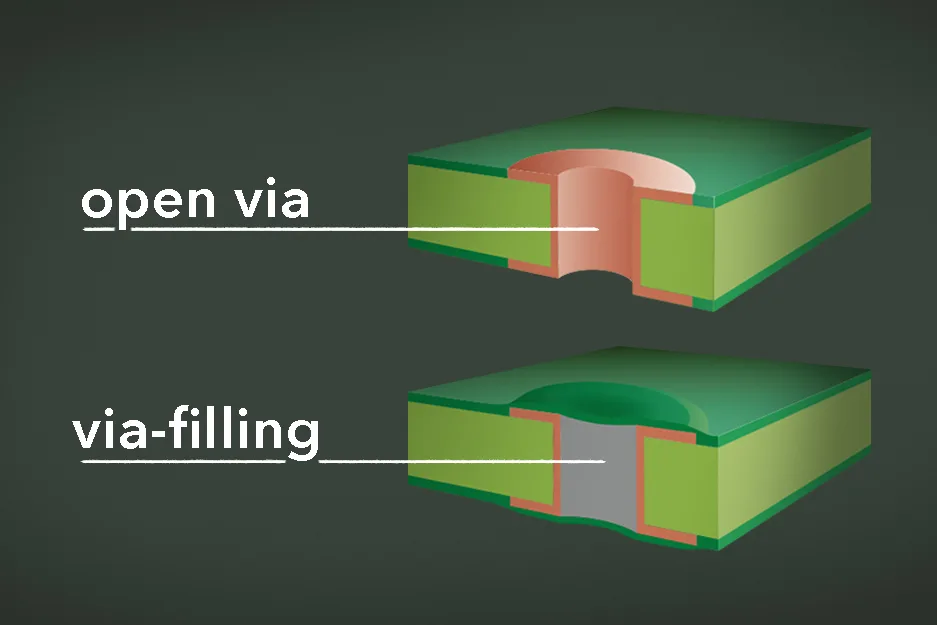
When we talk about Via Filling in PCBs, we refer to a filling process of vias holes with materials such as dielectric or isolating for various purposes. These include protecting hole metallization, preventing the passage of liquid or gas, impeding the way up of tin during wave soldering, and avoiding flows of resin when coating one side of the board. Different procedures can be used to obtain such seals, leading to different results. JHYPCB offers two possibilities – PSR Via Fill and Resin Via Fill, each with their unique sealing techniques.
The PSR Via Fill technique involves vias sealing through extra solder resist application using a dedicated drawing of solder mask. On the other hand, the Resin Via Fill technique involves obtaining sealing through specific epoxy resin application, considering the need for an over-coverage of metallic or solder resist material.
The PCB Via Filling process can also be done with either solder resist or resin, depending on the drilled diameter size. For drilled diameters lower or equal to 0.4mm, filling with solder resist is recommended, while filling with resin is suggested for diameters up to 0.7mm. However, for drilled diameters greater than 0.4mm, hole sealing is not guaranteed with solder resist as the material may create some problems during soldering. Similarly, even with lower drilled diameters, the usual loss of volume of the employed material during its polymerization can result in material gaps/voids/cracks inside holes.
PCB production often begins with a “core,” which is a simple double-sided PCB. Additional layers beyond the first two are stacked on top of this basic building block. When two more layers are consecutively stacked from the bottom core, various types of vias can be created, including 1-2 vias, 1-3 vias, and through holes. Each type of via is created by drilling at each stacking stage. When one layer is stacked on top of the core and another layer is stacked from the bottom, different via configurations become possible, including 1-3, 2-3, and through holes.
To determine the allowable stacking methods and via configurations for a particular PCB manufacturer, users must gather information about their specifications. For more cost-effective boards, only through holes may be created, while antipads or clearance areas may be placed on layers where vias should not be connected.
PCB via hole tolerance refers to the acceptable deviation in size and position of a via hole on PCB. Via holes are drilled holes in the PCB that are filled with metal, allowing for electrical connections between different layers of the board.
The tolerance for via holes will depend on the specific requirements of the PCB design and manufacturing process. The tolerance may be specified as a minimum and maximum diameter for the hole, as well as a maximum deviation in position from the original design location.
Typically, the tolerance for via hole diameter is around +/- 0.05mm to +/- 0.1mm, depending on the size of the via hole. The tolerance for position deviation may be specified in terms of the distance from the original location or as a percentage of the finished board size.
It is important to adhere to the specified tolerance limits for via holes, as deviations can impact the connectivity and functionality of the circuit board. A smaller hole than specified can lead to electrical resistance and potentially cause overheating, while a larger hole can impact the mechanical stability of the board.
To inspect the via quality of a printed circuit board, several aspects can be examined. Firstly, the via size and shape should be inspected to make sure that they are within the tolerances specified in the design files. This can be checked using a microscope or a digital camera with high magnification capabilities.
Secondly, the plating quality of the via should be checked. This can be done by examining the via walls and bottoms to make sure that they are evenly coated with copper. Any areas where the plating is missing or uneven can indicate a defect.
Thirdly, the via’s connection to the other layers of the board should be checked. This can be done by inspecting the board under a microscope, looking for any signs of delamination or separation between the layers.
Fourthly, using Cross-section to Examine Via Quality. By analyzing the cross-section, we can visually inspect the thickness of the via’s copper walls and measure the depth of any blind microvias. This enables a comprehensive evaluation of the via’s quality.
Finally, the via’s electrical connectivity can be tested using a multimeter or continuity tester. This can help to identify any shorts or open circuits in the via.
Overall, a thorough inspection of the via quality is important to ensure the reliability and performance of the printed circuit board.
Vias are an essential component of the PCB board that allows electrical and thermal energy to move from layer to layer. To facilitate this, more vias should be used for parts of the circuit carrying power or fast signals. It is generally better to use several smaller vias than one large via as it reduces inductance and provides additional paths for current in case one of the vias fails.
For a double-sided board, a through-hole via is the only option. However, for multilayer PCBs, blind or buried vias can also be specified at an increased cost. Through-hole vias can result in an unused hole (and possibly an unused pad), consuming PCB real estate and interfering with routing on adjacent layers. Still, they are the cheapest and most reliable option when a via needs to form an electrical connection between internal and external layers. Blind vias, in contrast, can free up real estate by creating a connection between the two layers and a hole only on the layers in between. While buried vias are not often used due to expense, reliability concerns, and difficulty of troubleshooting.
Our approach to manufacturing blind and/or buried vias involves a combination of depth-controlled laser drilling and mechanical NC drilling. For standard PCBs and HDI PCBs, the capabilities of our blind and buried vias manufacturing are as follows.
Via holes are small tunnels or holes drilled through a printed circuit board (PCB) from one layer to another. They provide electrical connectivity between different layers of a PCB.
There are different types of via holes, such as through-hole via holes, blind via holes, and buried via holes. Through-hole via holes extend through the entire thickness of the board, while blind via holes only extend through a few layers and buried via holes are completely covered by other layers.
Via holes are made by drilling small holes in a PCB using a drill bit or a laser. The holes are then plated with copper to create an electrical connection between different layers of the PCB.
Factors that should be considered when designing PCB via holes include the size and depth of the hole, the location of the hole, the amount of current that will pass through the hole, the type of plating used, and the cost.
Via holes help to reduce the size of a PCB by allowing multiple connections to be made between layers, thus increasing the density of components on the board. They also provide a more reliable and efficient way to transfer electrical signals between different layers of the board.
Some common problems that can occur with via holes on a PCB include insufficient plating, misaligned holes, drill bit breakage, and excessive heat buildup during the plating process. These issues can lead to poor electrical performance and reliability of the PCB.
Via hole problems can be addressed by ensuring that a proper plating process is used, selecting the appropriate drill bit size and shape, using high-quality materials, and performing thorough testing and inspection of the board.
Whether you need additional via holes for high-power or high-speed circuits depends on the specific design requirements of your circuit. In general, high-speed circuits may require additional via holes to reduce signal reflection, minimize ground bounce, and reduce noise. For high-power circuits, via holes may be needed to improve heat dissipation and prevent thermal issues. However, additional via holes can add complexity and cost to your design, so it's important to carefully weigh the benefits and drawbacks before making a decision.
The cost associated with different types of via holes can vary based on several factors, including the number of vias needed, the size of the vias, and the type of via used. Here are some general guidelines:
Through-hole via: This is the most common type of via, and it typically costs less than other types of vias. They are suitable for most applications where the PCB is not too complex.
Blind via: A blind via is drilled from the outer layer of the PCB to an inner layer, but it doesn't go all the way through to the opposite side. Blind vias can reduce the overall layer count, enabling more density in your PCB, but they can be more expensive than traditional through-hole vias.
Buried via: A buried via is drilled between two inner layers of the PCB and doesn't extend to the outer layers. Buried vias are more difficult and expensive to manufacture than through-hole vias.
Micro via: These vias are very small in size and can save space in the PCB design and allow for higher routing density. However, they are more expensive than regular through-hole vias.
Ultimately, the cost of via holes will depend on your specific design requirements and the capabilities of your manufacturing process.
Yes, you can use multiple small vias instead of one large via in your PCB design. This technique is called "via stitching" or "via-in-pad." When you use multiple small vias, the current can be spread out more evenly, reducing the thermal load on each via and ensuring better performance.
Via stitching involves placing multiple small vias within the pad of a surface-mount component or along a trace. These small vias act as a network of conductive paths that distribute current and minimize the resistance of the circuit. When designing via stitching, it is important to consider the size, spacing, and number of vias required for the application you are working on.
Using multiple small vias typically requires more board area. However, this approach can provide additional benefits such as improved electrical performance, better heat dissipation, and increased reliability.
There are several ways in which you can optimize the via placement in your PCB design to minimize signal loss and improve signal quality.
Place vias near the source and load components: Vias placed close to the source and load components can minimize the length of the trace, reducing signal losses.
Use vias with shorter stub lengths: Stubs, or the lengths of the via that extend beyond the trace, can cause signal reflections. Using vias with shorter stub lengths can reduce these reflections and improve signal quality.
Place vias away from high-speed signal traces: Via placement near high-speed signal traces can cause signal crosstalk and interfere with signal quality. Placing vias a safe distance away from these high-speed traces can minimize their impact.
Use via stitching: Via stitching can improve signal quality by distributing current more evenly across the board and reducing the resistance of the circuit.
Place vias in a regular pattern: Placing vias in a regular pattern can reduce the chance of resonance and improve signal quality.
Use via shielding: Shielding a via by surrounding it with ground vias can reduce electromagnetic interference (EMI) and improve signal quality.
Consider the signal frequency: The optimal via placement may vary depending on the frequency of the signal being transmitted. High-frequency signals may require a different via placement than low-frequency signals.
Ultimately, the optimal via placement strategy will depend on the specific requirements of your PCB design, including the type of circuit, the components used, and the operating conditions.
Yes, via holes can carry both electrical and thermal loads. They are commonly used in printed circuit board designs as a means of transferring heat from one layer of the board to another or from the board to a heat sink. They can also be used to carry electrical signals between different layers of the board. However, it is important to note that the size, shape, and placement of the vias can have an impact on their ability to carry both electrical and thermal loads, so careful design considerations are necessary.
The size and number of via holes required for a PCB design depend on a variety of factors, including:
Current density: The size and number of via holes should be chosen based on the amount of current density that will run through the via. Larger current densities require larger via holes.
Thermal management: The size and number of via holes can help improve heat transfer in a board. A large number of small vias can help increase the surface area for heat transfer.
Signal integrity: The size and number of via holes can impact signal integrity. It is important to minimize the number of vias for critical high-speed signals to reduce signal loss.
PCB layer count: The number of PCB layers can impact the size and number of via holes. More layers may require more vias to connect different layers.
Cost: The size and number of via holes can impact the cost of the PCB. Smaller vias are more expensive and can increase the overall cost of the board.
Manufacturing limitations: It is important to consider the capabilities of the manufacturing process when selecting the size and number of via holes. Smaller via holes may require more expensive manufacturing techniques.
By considering these factors and carefully selecting the size and number of via holes, you can improve the performance and reliability of your PCB design.
Calculating the via diameter and clearance involves considering several factors such as the current density, thermal management, signal accuracy, and the number of layers in the PCB, among others.
One common approach is to use the IPC-2221 standard. This standard provides guidelines for via hole sizes based on the current carrying capacity needed. You can also refer to the manufacturer's datasheets for recommendations on via sizes and clearances based on their specific materials and manufacturing capabilities.
For example, for a via with a current of 1A, the IPC-2221 recommends a hole size of 0.45mm and a clearance of 0.25mm. However, it is important to note that these values may vary depending on the specific design and manufacturing process.
Additionally, thermal management requirements will play a significant role in determining the via diameter and clearance. This is especially important for high-power designs where heat dissipation is critical. In such cases, larger vias with wider clearances might be necessary to manage heat more effectively.
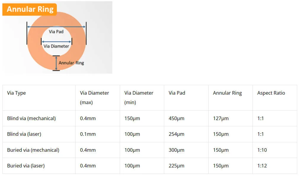
Annular ring is the area of copper that surrounds a drilled hole on a printed circuit board. It is the amount of copper that remains after a hole has been drilled in the PCB. The size of the annular ring is important as it affects the electrical and mechanical properties of the PCB. It is recommended to maintain a certain amount of annular ring to ensure proper contact between through-hole components and the PCB pads. The annular ring is typically specified as a distance between the center of the through-hole and the edge of the copper pad.
The aspect ratio of a via on a printed circuit board (PCB) is the ratio of the hole diameter to the thickness of the board that the via passes through. Aspect ratio is an important design consideration because it can have a significant impact on the manufacturability, reliability, and functionality of a PCB. The aspect ratio can affect the plating thickness of the via, the quality of the solder mask, the risk of drill breakage during fabrication, and the electrical performance of the via.
To ensure proper fabrication and functionality of a PCB, it is important to design the aspect ratio within acceptable limits for the specific fabrication process being used. The acceptable aspect ratio range may vary depending on factors such as the thickness and material of the board, the diameter of the via, and the plating process used. Typically, the aspect ratio range is between 1:1 to 10:1, with smaller ratios being easier to manufacture. It is always recommended to consult the PCB fabricator for their specific aspect ratio requirements before designing a PCB.
When you partner with us, we do everything to ensure your PCB manufacturing and assembly are completed on time to your specifications with the highest quality.
Fill out the form below, and we will get back to you within the next 24
hours to complete the order, and then you’re all set to get started!