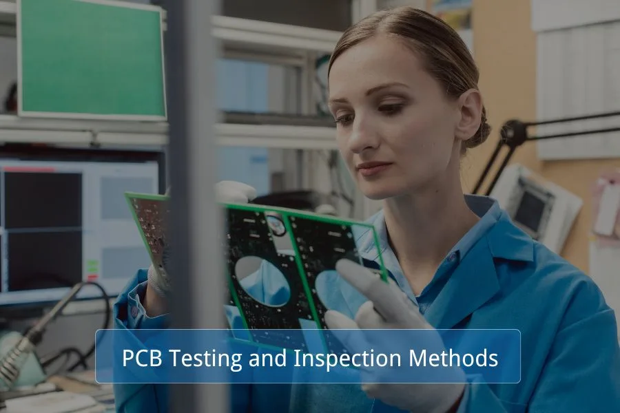
PCB Quality Assurance

PCB Testing and Inspection: Ensuring Quality at Every Step

Discover how our rigorous testing processes and cutting-edge inspection techniques ensure the reliability and performance of every PCB we produce, setting the industry standard for quality assurance.

At JHYPCB, we understand that the reliability and performance of your electronic products hinge on the quality of their printed circuit boards (PCBs). That’s why we’ve implemented a rigorous testing and inspection regime that scrutinizes every PCB at multiple stages of production. Our commitment to quality isn’t just a promise – it’s a meticulous process that combines cutting-edge technology with human expertise. In this guide, we’ll walk you through our comprehensive PCB testing and inspection methods, demonstrating how we ensure that every board that leaves our facility meets the highest standards of excellence.

PCB_Testing_and_Inspection_Methods

Visual Inspection Techniques

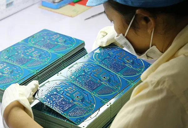
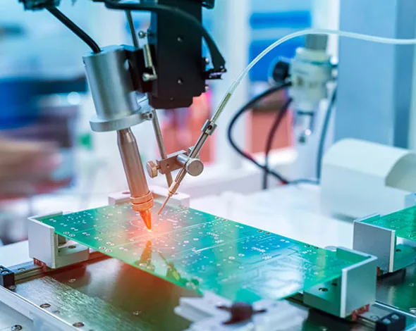
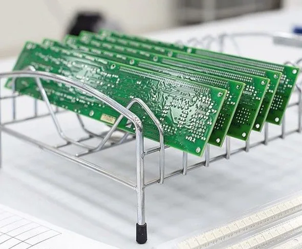
Visual inspection forms the foundation of our quality control process. It’s often the first line of defense against defects and plays a crucial role in identifying issues that may be missed by automated systems. At JHYPCB, we employ both manual and automated visual inspection techniques to ensure no detail goes unnoticed.

Manual Visual Inspection

Our skilled technicians perform thorough manual visual inspections at various stages of the PCB manufacturing process. This hands-on approach allows us to detect a wide range of potential issues:

  • Surface defects: We check for scratches, dents, or other physical damage to the board surface.
  • Solder mask and silkscreen quality: Our inspectors verify the correct application and alignment of solder mask and silkscreen printing.
  • Hole quality: We examine drilled holes for proper size, position, and absence of burrs.
  • Copper trace integrity: Technicians look for any breaks, thinning, or other irregularities in copper traces.
  • Component placement and orientation: For assembled boards, we ensure all components are correctly placed and oriented.
  • Solder joint quality: Our experts assess each solder joint for proper formation and absence of defects like bridging or insufficient solder.

The advantage of manual inspection lies in the human eye’s ability to detect subtle anomalies and patterns that might escape automated systems. Our inspectors are trained to spot even the slightest deviations from specifications, ensuring that only the highest quality PCBs proceed to the next stage of production.

Manual Visual Inspection of PCBs
PCB Visual Inspection

Automated Optical Inspection (AOI)

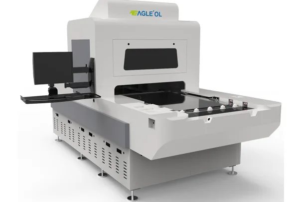
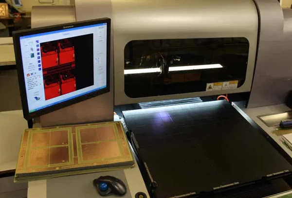
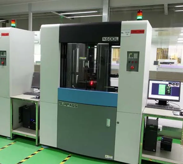
To complement our manual inspections and handle high-volume production with consistency, we utilize state-of-the-art Automated Optical Inspection (AOI) systems. Here’s how our AOI process works:

  1. High-resolution imaging: The AOI machine captures detailed images of the PCB using high-resolution cameras and specialized lighting.
  2. Image analysis: Advanced software compares these images against a “golden” reference board or CAD data.
  3. Defect detection: The system identifies potential defects such as:
    • Missing or misaligned components
    • Solder bridges or insufficient solder
    • Component polarity issues
    • Incorrect component values
    • Copper trace defects
    • Solder mask imperfections
  4. Reporting: The AOI system generates detailed reports, highlighting any detected anomalies for further review.
  5. Human verification: Our technicians review flagged issues to confirm true defects and eliminate false positives.

The AOI system excels at rapidly inspecting large quantities of PCBs with a high degree of accuracy and consistency. It can detect defects as small as 0.5mm, ensuring that even minute issues are caught and addressed.

By combining the speed and precision of AOI with the nuanced judgment of manual inspection, JHYPCB creates a robust visual inspection process that catches defects early, reduces waste, and ensures that only top-quality PCBs move forward in the production process.

Our commitment to thorough visual inspection is just the beginning of our comprehensive quality assurance process. In the following sections, we’ll explore the additional testing methods we employ to guarantee the electrical integrity and overall reliability of your PCBs.

PCB AOI System
PCB AOI Inspection

Electrical Testing Methods

While visual inspection is crucial, it’s equally important to verify the electrical integrity of each PCB. At JHYPCB, we employ a variety of electrical testing methods to ensure your boards function as intended.

Continuity and Isolation Testing

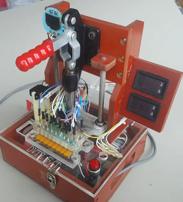
Continuity and isolation testing form the backbone of our electrical verification process. This fundamental test serves two critical purposes:

  1. Continuity Testing: We verify that all intended connections on the PCB are properly made. This ensures that every trace, via, and pad that should be connected is indeed electrically continuous.
  2. Isolation Testing: We check that there are no unintended connections or short circuits between independent nets on the board.

Process:

  • Our advanced testing equipment applies a small voltage across various points on the PCB.
  • For continuity, we measure the resistance between points that should be connected, ensuring it falls below a specified threshold.
  • For isolation, we check that the resistance between independent nets is above a certain threshold, typically in the megaohm range.

This testing method helps us identify issues such as open circuits, short circuits, and manufacturing defects that might not be visible to the naked eye.

Flying Probe Testing

For prototype runs, small batches, or complex boards, we utilize flying probe testing. This flexible method offers several advantages:

  • How it works: Computer-controlled probe heads move rapidly across the board, making contact with test points to perform electrical measurements.
  • Versatility: Flying probe testers can easily adapt to different board designs without requiring custom fixtures.
  • Comprehensive testing: It can perform continuity, isolation, component, and even basic functional tests.
  • High precision: Our flying probe systems can access test points as small as 0.1mm, making them ideal for high-density boards.

The flexibility of flying probe testing allows us to quickly set up tests for new or revised designs, reducing time-to-market for your products.

Flying Probe Test Machine
PCB Bed of Nails Test Fixture

Bed of Nails Testing

For high-volume production runs, we employ bed of nails testing, also known as in-circuit testing (ICT). This method is highly efficient and thorough:

  • Custom fixture: We create a dedicated test fixture with spring-loaded pins (the “nails”) that make contact with predetermined test points on your PCB.
  • Simultaneous testing: The bed of nails can test multiple points simultaneously, dramatically reducing test time compared to flying probe testing.
  • Comprehensive checks: Beyond basic continuity and isolation, bed of nails testing can verify component values, test analog and digital circuits, and even perform basic functional tests.
  • High-speed testing: Once set up, this method can test hundreds of boards per hour, making it ideal for large production runs.

While the initial setup time for bed of nails testing is longer due to fixture creation, it provides unparalleled efficiency and thoroughness for high-volume manufacturing.

Specialized PCB Tests

In addition to standard electrical tests, JHYPCB offers a range of specialized tests to ensure your PCBs meet specific performance requirements and industry standards.

Impedance Testing

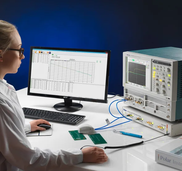
For high-speed digital circuits and RF applications, controlling impedance is crucial. Our impedance testing process ensures your boards meet the exact specifications required:

  • Time-Domain Reflectometry (TDR): We use advanced TDR equipment to measure the impedance of traces along their entire length.
  • Accuracy: Our systems can measure impedances with an accuracy of ±1 ohm.
  • Customized testing: We can test for specific impedance values (e.g., 50 ohm, 75 ohm, 100 ohm) as required by your design.
  • Documentation: Detailed impedance reports are provided, allowing you to verify compliance with your specifications.

By carefully controlling impedance, we help ensure signal integrity in your high-performance electronic products.

PCB Impedance Testing
PCB Solderability Testing

Solderability Testing

Proper solderability is essential for reliable assembly and long-term product durability. Our solderability testing includes:

  • Wetting balance test: We measure the wetting force and speed to ensure optimal solder joint formation.
  • Solder float test: This test verifies the ability of plated holes to withstand soldering temperatures without degradation.
  • X-ray fluorescence (XRF) analysis: We use XRF to measure the thickness and composition of surface finishes, ensuring they meet specifications for reliable soldering.

These tests help prevent assembly issues and ensure your PCBs will form strong, reliable solder joints during the assembly process.

Cleanliness Testing

PCB cleanliness is critical for long-term reliability, especially in harsh environments or high-voltage applications. Our cleanliness testing includes:

  • Ionic contamination testing: We use specialized equipment to measure the level of ionic contaminants on the board surface.
  • Resistivity of Solvent Extract (ROSE) testing: This method quantifies the overall cleanliness of the PCB.
  • Visual inspection under UV light: This helps identify any organic contaminants that might not be visible under normal lighting.

By ensuring your PCBs meet stringent cleanliness standards, we help prevent issues such as electrochemical migration, dendritic growth, and corrosion, all of which can lead to premature product failure.

PCB Cleanliness Testing

Through these specialized tests, JHYPCB goes beyond basic quality control to ensure your PCBs meet the highest standards of performance and reliability. Our comprehensive testing regime gives you the confidence that your boards will function as intended, even in the most demanding applications.

Reliability and Stress Testing

At JHYPCB, we understand that your PCBs need to perform reliably not just at the time of manufacture, but throughout the entire lifecycle of your product. That’s why we conduct rigorous reliability and stress testing to ensure your boards can withstand real-world conditions.

Thermal Stress Testing

Electronic components and PCBs often operate in environments with fluctuating temperatures. Our thermal stress testing simulates these conditions to verify the long-term reliability of your boards:

  • Thermal Cycling: We subject PCBs to repeated cycles of extreme high and low temperatures, typically ranging from -65°C to +125°C. This test reveals any weaknesses in solder joints, plated-through holes, and overall board construction.
  • Thermal Shock: This more aggressive test rapidly changes the temperature, stressing the board and components to their limits. It’s particularly effective at identifying potential delamination issues or problems with the coefficient of thermal expansion (CTE) mismatches.
  • High-Temperature Operating Life (HTOL): We expose the PCBs to elevated temperatures while under electrical bias for extended periods. This accelerated aging test helps predict long-term reliability.

Microsection Analysis

While this is a destructive test, microsection analysis provides invaluable insights into the internal structure and quality of your PCBs:

  1. Sample Selection: We carefully select representative samples from your production run.
  2. Cross-Sectioning: The selected boards are precisely cut to expose the areas of interest.
  3. Polishing: The exposed surfaces are finely polished to achieve a mirror-like finish.
  4. Microscopic Examination: Using high-powered microscopes, our technicians examine:
    • Plated-through hole quality and copper distribution
    • Layer-to-layer registration
    • Innerlayer bond quality
    • Solder mask adhesion
    • Component solder joint quality (for assembled boards)
  5. Measurements: We take precise measurements of critical features like plating thickness, dielectric spacing, and via structures.
  6. Documentation: Detailed reports with microscopic images and measurements are provided, offering a comprehensive view of your PCB’s internal quality.

This analysis allows us to verify the internal structure of your PCBs, ensuring they meet IPC standards and your specific requirements. It’s an essential tool for process control and continuous improvement of our manufacturing techniques.

Microsection Inspection

Our PCB Testing Process

At JHYPCB, quality assurance is not a single step but an integral part of our entire manufacturing process. Here’s an overview of how we integrate testing and inspection throughout PCB production:

Incoming Material Inspection:

  • We test all raw materials, including copper-clad laminates, prepregs, and chemicals, to ensure they meet our stringent quality standards.
  • X-ray fluorescence (XRF) analysis is used to verify the composition and thickness of copper foils.

My Artwork and Drilling Verification:

  • Our CAM engineers carefully review and verify all customer data.
  • We perform DFM (Design for Manufacturability) analysis to identify and address potential issues before production begins.

Inner Layer Processing:

  • AOI is used to inspect inner layers for defects after imaging and etching.
  • We perform electrical testing on inner layers to catch any continuity or isolation issues early in the process.

Lamination Quality Check:

  • After lamination, we use ultrasonic thickness measurement to ensure uniform thickness across the board.
  • X-ray inspection is employed to verify the alignment of inner layers and the quality of buried vias.

Drilling and Plating Inspection:

  • We use sophisticated measurement tools to verify hole sizes and positions.
  • Cross-sections are analyzed to check plating thickness and quality.

Outer Layer Processing:

  • AOI is again used to inspect outer layers after imaging and etching.
  • We perform manual visual inspection to catch any defects that AOI might miss.

Solder Mask and Legend Application:

  • UV light inspection is used to check solder mask coverage and adhesion.
  • We visually inspect legend quality and alignment.

Surface Finish Application:

  • XRF analysis is used to verify the thickness and quality of the surface finish (e.g., ENIG, HASL, Immersion Tin).
  • We perform solderability testing to ensure reliable assembly.

Electrical Testing:

  • Every board undergoes electrical testing (flying probe or bed of nails) to verify continuity and isolation.
  • Impedance testing is performed on controlled impedance boards.

Final Inspection:

  • We conduct a thorough visual and dimensional inspection of finished boards.
  • Cleanliness testing is performed to ensure boards meet IPC standards.

Reliability Testing:

Sample boards from each lot undergo thermal stress testing and microsection analysis as per customer requirements or our internal quality control procedures.

Packaging and Shipping:

  • We perform a final visual check during packaging to ensure boards are properly protected for shipping.
  • Each shipment includes a detailed Certificate of Conformance summarizing all tests performed and results.

This comprehensive testing process ensures that every PCB leaving our facility meets the highest quality standards. We maintain detailed records of all test results, providing full traceability and allowing us to continuously refine our processes for even better quality and reliability.

At JHYPCB, we’re not just manufacturing PCBs – we’re crafting the foundation of your electronic products with precision, care, and an unwavering commitment to quality.

Quality Assurance Standards

At JHYPCB, we don’t just aim to meet industry standards – we strive to exceed them. Our commitment to quality is reflected in our adherence to and implementation of globally recognized standards:

  • IPC-A-600: We rigorously follow this standard for acceptability of printed circuit boards. Our inspectors are IPC-A-600 certified, ensuring they can identify and classify PCB imperfections according to industry-accepted criteria.
  • IPC-6012: This standard for rigid PCBs guides our qualification and performance specifications. We ensure our boards meet or exceed these requirements for all performance classes.
  • ISO 9001:2015: Our quality management system is certified to ISO 9001:2015, demonstrating our commitment to consistent quality and continuous improvement.
  • IPC-J-STD-001: For PCB assembly, we adhere to this standard for soldered electrical and electronic assemblies.
  • AS9100D: For our aerospace and defense customers, we maintain AS9100D certification, meeting the stringent quality requirements of these industries.

By aligning our processes with these internationally recognized standards, we ensure that our PCBs meet the highest quality benchmarks across various industries and applications.

Benefits of Comprehensive PCB Testing

Investing in thorough PCB testing and inspection offers numerous advantages for our customers:

  • Enhanced Reliability: Rigorous testing identifies potential issues before they become problems in your final product, leading to more reliable end-products and fewer field failures.
  • Cost Savings: While comprehensive testing may seem costly upfront, it significantly reduces expenses associated with product recalls, warranty claims, and reputation damage in the long run.
  • Faster Time-to-Market: By catching and resolving issues early in the production process, we help you avoid delays in your product development and launch cycles.
  • Regulatory Compliance: Our testing processes ensure your PCBs meet industry standards and regulatory requirements, simplifying your product certification process.
  • Performance Optimization: Through specialized tests like impedance testing, we help ensure your PCBs perform optimally in high-speed and high-frequency applications.
  • Quality Assurance: Our multi-stage testing process provides you with confidence in the quality and functionality of every PCB we produce.
  • Continuous Improvement: The data gathered from our comprehensive testing allows us to continuously refine our manufacturing processes, leading to ever-improving quality and yields.
  • Traceability: Our detailed test records provide full traceability, which is crucial for many industries and can be invaluable in the rare event of a quality issue.

FAQs about PCB Testing and Inspection

We maintain a strict calibration schedule for all our testing equipment, following manufacturer guidelines and industry standards. Our equipment is regularly verified against certified reference standards.

Absolutely! We understand that different applications may require unique testing protocols. Our engineering team can work with you to develop and implement custom tests tailored to your specific needs.

If a board fails any test, it is immediately flagged and isolated. Our quality team investigates the cause of the failure, implements corrective actions, and determines if any other boards in the lot may be affected. We then retest to ensure the issue has been resolved.

Yes, we provide comprehensive test reports with every order. These reports detail the tests performed, the results, and any relevant measurements or observations.

For high-reliability applications, we implement additional testing protocols and often increase sampling rates. We can also provide full lot testing if required. Our AS9100D certification demonstrates our capability to meet the stringent requirements of aerospace applications.

Contact us Today

At JHYPCB, we believe that quality is not just about meeting specifications—it’s about exceeding expectations. Our comprehensive PCB testing and inspection processes are the cornerstone of our commitment to delivering PCBs that you can trust implicitly. From the moment raw materials enter our facility to the final inspection before shipping, every step of our manufacturing process is scrutinized to ensure the highest quality standards are met.

We understand that your PCBs are critical components in your products, and their reliability directly impacts your success. That’s why we invest heavily in state-of-the-art testing equipment, rigorous processes, and continuous training for our staff. When you choose JHYPCB, you’re not just getting a PCB manufacturer—you’re gaining a partner committed to the quality and success of your products.

Ready to experience the JHYPCB difference? Contact us today to discuss your PCB needs or to request a quote. Let us show you how our meticulous testing and inspection processes can give you the confidence and peace of mind you deserve in your PCB supplier. Together, we’ll build the foundation for your next groundbreaking electronic product.

Related Reading

Scroll to Top

Request A Quote

Let’s Do This!

Fill out the form below, and we will get back to you within the next 24
hours to complete the order, and then you’re all set to get started!