


Your Trusted Prototype PCB Manufacturing And Assembly Partner.
When you partner with us, we do everything to ensure your PCB manufacturing and assembly are completed on time to your specifications with the highest quality.
Leading manufacturer of PCB Fabrication and Assembly in China.
Welcome to JHYPCB, your premier source for high-quality single-sided and single-layer PCBs in China. With over 10 years of experience manufacturing PCBs, JHYPCB specializes in producing top-notch single-sided and single-layer boards for clients worldwide.
Our single-sided PCBs feature copper traces on only one side of the board, while our single-layer PCBs have copper traces throughout a single layer. Both provide a cost-effective solution for simple circuit designs and prototyping needs.
At JHYPCB, we utilize cutting-edge facilities and equipment to fabricate single-sided and single-layer PCBs to your exact specifications. Our rigorous quality control standards ensure your boards are expertly crafted and thoroughly tested.
Whether you need quick-turn prototypes or medium-sized production runs, JHYPCB has the capabilities to deliver high-quality single-sided and single-layer PCBs on time and on budget. We offer competitive pricing with no hidden fees.
Contact us today to learn more about our single-sided and single-layer PCB fabrication services. Our team of engineers is ready to answer any questions and help you get your project started on the right track.
Single-sided or single-layer printed circuit boards provide an affordable solution for basic circuit and prototype designs.
A single-sided PCB has copper traces on only one side of the board. Components are mounted on the same side as the copper traces. Single-sided PCBs work well for simple layouts with minimal component placement needs. They allow traces to run uninterrupted without the need for drilling or plating through holes.
A single-layer PCB has copper traces throughout the entire area of one board layer. While physically a double-sided board, electrically it functions as a single-layer board because traces exist on one signal layer only. Single layer boards accommodate more complex tracing while still being cost-effective for moderate complexity designs.
The main advantages of single-sided and single-layer PCBs include:
Single-sided and single-layer PCBs meet the needs of many hobby, academic, and commercial electronic projects. Their simplicity, cost-effectiveness, and quick turnaround times make them an attractive option for creating a functioning circuit board.
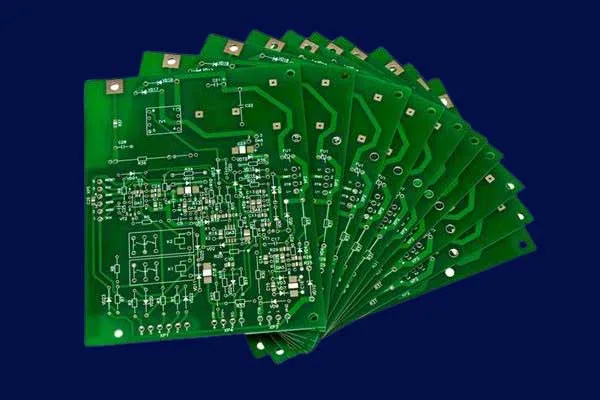
A bare single-sided PCB sample with a green solder mask
With over 10 years of experience manufacturing printed circuit boards, JHYPCB has honed our process to deliver exceptional quality single-sided and single-layer PCBs. We utilize cutting-edge facilities equipped with the latest fabrication and assembly technologies to produce boards that meet and exceed our customers’ expectations.
Our factory employs advanced PCB equipment from industry leaders like Orbotech and Atg. This enables us to create precision boards with fine line traces and spacing down to 3 mil, wrap-around plating, and other demanding fabrication requirements.
We follow strict quality control standards at every stage of production. From incoming raw material inspection to solder mask cure verification, we carefully examine PCBs to ensure consistent quality. We can reliably produce boards from run to run with the highest degree of repeatability.
For every order, we collaborate closely with customers to understand their design needs and specifications. Our engineers provide knowledgeable guidance to optimize the board layout for manufacturability and performance. Once the design is finalized, we fabricate the PCBs according to the customer’s exact specifications.
In addition to prototyping services, JHYPCB has the volume production capacity to handle orders ranging from a few boards up to 10,000 boards. We can accommodate small prototype orders within 24 hours as well as medium-sized production runs, with standard lead times of 5 days for production.
Our pricing is highly competitive, with no hidden fees. As a full-service PCB solutions provider, JHYPCB delivers exceptional quality single-sided and single-layer boards with responsive customer service, expert technical assistance, and transparency in pricing. Contact us today to experience the JHYPCB difference!
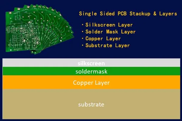
The single-sided PCB stackup refers to the arrangement of layers in a single-sided PCB. It typically consists of three layers:
The substrate layer, which is the base material of the PCB.
The conductive layer, which is the layer that contains the conductive pathways.
The protective layer, which is the top layer that protects the conductive pathways from environmental damage.
Read More: PCB Layers Explained: Multilayer PCB Stakcup
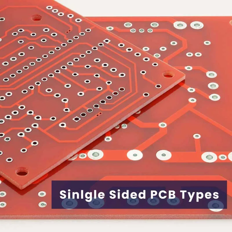
Here are the main types of single layer PCBs:
So in summary, there are several construction methods and substrate materials to choose from when designing a single layer PCB depending on the design requirements and constraints.
Here are some potential disadvantages of using a single layer PCB design:
While disadvantages exist, single layer boards provide a simple and low-cost solution when the circuit complexity and performance requirements are relatively basic. For more advanced designs, multilayer boards are likely needed.
Here are some tips for designing an effective single-layer PCB:
With careful planning and optimization, it is possible to successfully implement many design circuits using a simple single-layer PCB layout. Prototyping on single-layer boards can help verify a design before moving to multilayer.
Single-layer PCBs are typically made from a combination of different materials, including:
Conductive material: The conductive material is typically made of copper and is used to create the conductive pathways on the PCB.
Protective material: The protective material is used to cover the conductive pathways and protect them from environmental damage. This material is usually a resin or lacquer.
Read More: Complete Guide for PCB Material
Here are some of the common applications for single-sided PCBs:
So in summary, single-sided PCBs are the most cost-effective choice for any non-complex low-frequency electronics device or design. Their simple construction makes them ideal for fast prototyping iterations.
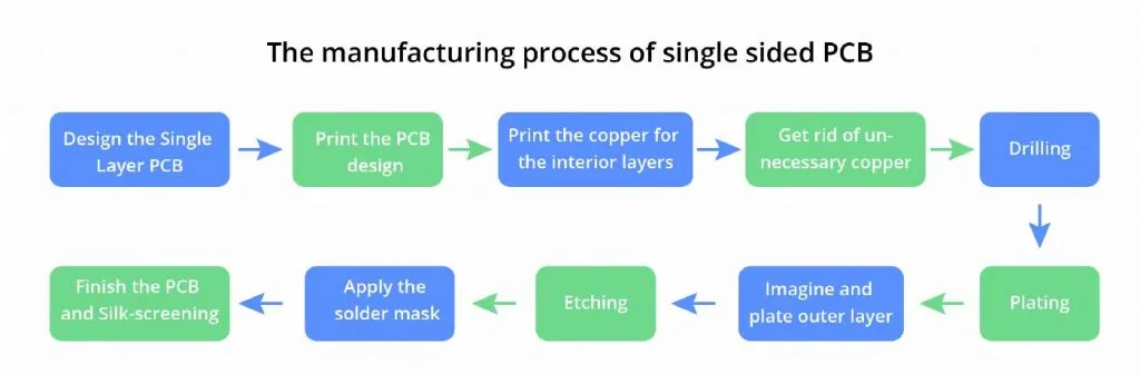
Single-sided PCBs are manufactured using a photolithography process, which involves the following steps:
Preparing the substrate: The substrate material is cut to size and cleaned to remove any contaminants.
Depositing the conductive material: The conductive material is deposited onto the substrate using a deposition process, such as electroplating.
Patterning the conductive material: The conductive material is patterned using photolithography techniques to create the conductive pathways.
Applying the protective material: The protective material is applied over the conductive pathways to protect them from environmental damage.
At JHYPCB, we provide a comprehensive range of printed circuit board solutions beyond just single-sided and single-layer boards. We have extensive experience in manufacturing:
We support the most demanding PCB design requirements, including high layer counts, blind and buried vias, controlled impedance, and heavy copper boards. Our engineering team has extensive experience across a wide range of end products – from telecommunications boards to auto electronics to industrial control systems.
Whether you need just a few prototype boards or full-scale mass production, we deliver. Our quick-turn prototyping services enable 1-day turnaround for 10 boards. The production runs from small batches of 10 boards to larger quantities of 10,000+ boards are easily accommodated.
With JHYPCB as your trusted PCB solutions partner, you have a one-stop resource to bring your designs from concept to high-volume manufacturing.
The cost of single-layer PCBs varies depending on several factors, including the size of the PCB, the number of components, and the materials used. However, single-layer PCBs are typically cheaper than multi-layer PCBs, making them a more cost-effective option for low-complexity electronic devices.
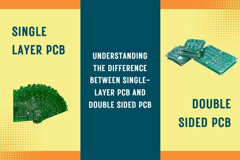
The main difference between single-layer and double-sided PCBs is that single-layer PCBs have conductive pathways on one side of the board only, while double-sided PCBs have conductive pathways on both sides of the board. Double-sided PCBs are more complex and offer more functionality than single-layer PCBs.
Single-layer PCBs have conductive pathways on one side of the board only, while multilayer PCBs have conductive pathways on multiple layers within the board. Multilayer PCBs are more complex and offer more functionality than single-layer PCBs.
HASL, immersion silver, ENIG, and immersion tin are popular finish options.
FR-4 with 1oz (35 μm) copper is standard. Flex PCBs use polyimide. 1.6mm thickness is common.
When you partner with us, we do everything to ensure your PCB manufacturing and assembly are completed on time to your specifications with the highest quality.
Fill out the form below, and we will get back to you within the next 24
hours to complete the order, and then you’re all set to get started!