


Your Trusted Prototype PCB Manufacturing And Assembly Partner.
When you partner with us, we do everything to ensure your PCB manufacturing and assembly are completed on time to your specifications with the highest quality.
Leading manufacturer of PCB Fabrication and Assembly in China.
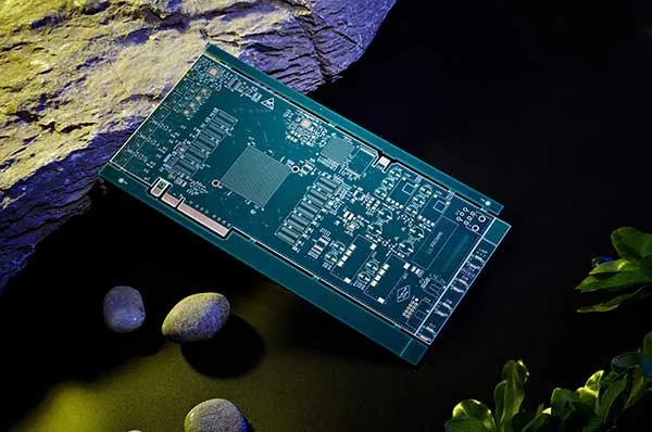
Nowadays, the circuitry requirement in most products and projects cannot be fulfilled by a simple single-layer or double-layer PCB. For complex situations and advanced performance, multilayer layer PCBs are essential. They ensure optimal performance, reduced size, and multiple benefits that create a massive demand in the industry.
As a leading multilayer PCB manufacturer, JHYPCB specializes in providing high-quality multilayer PCB manufacturing services to customers worldwide. With our advanced production equipment, experienced engineering team, and rigorous quality control system, we are capable of producing multilayer PCBs up to 64 layers with precision and efficiency. From prototyping to mass production, we are committed to delivering customized solutions and exceptional customer service to meet the unique needs of each client. Choose JHYPCB for your multilayer PCB manufacturing needs and experience reliable quality, competitive pricing, and timely delivery.

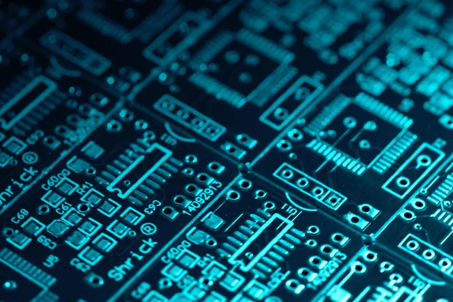
Any PCB that contains more than two conducting layers is called a Multilayer PCB. These layers are stacked one over the other, and there is an insulating or dielectric medium between them. If you look at a multilayer PCB, it will be just like a double-sided PCB, which means having components on both sides. However, the other layers will be underneath the components.
According to the requirements, the number of layers can be up to 64 layers or even more. All these conducting layers carry a signal, which can be adjusted according to the usage. Therefore, it can be used for complex operations. It offers better performance and reliability.
The structure of a multilayer PCB is quite simple. Stack one layer over the other, and there should be a suitable insulating medium, dielectric material, or prepreg to prevent short circuits between layers. In this way, the required number of layers is easily achieved.
The components are placed at the top and the bottom of the PCB, while the inside layers are only for conducting signals, which could be power, ground, and other signals required for the functioning. Therefore, inner layers are also often called routing layers.
Other than that, there are surface finishes, solder masks, and silkscreen at the front layers of the PCB.
Related Reading:

The connection of layers in a multilayer PCB is state-of-the-art technology. It is done through different types of vias.
A via is nothing but an electrical connection; however, it is very tiny. It connects the required layers of the PCB, even if they are internal layers. Consider it like a hole that is drilled to connect two or more layers.
There are three common types of vias.

This via is a through-hole from the top layer of the PCB to the bottom. It is like a drill hole, which is plated for conduction. It is usually done to connect all or multiple layers of the PCB.
A blind via is also a hole, but it does not pass through the entire board. It connects one outside layer to the inner layers of the PCB.
A buried via is buried inside the PCB. It connects the internal layers. You cannot see this via.
Learn More about What are the Benefits of Multilayer PCB?
At JHYPCB, we specialize in simple to complex multilayer PCBs according to the buyer’s requirements. You can get custom PCB prototypes and small-large volume PCB manufacturing at a reasonable cost. Without any limitation of MOQ, you can order prototypes and PCBs with fast shipment. Our experts are always ready to help you out in getting the best PCB that can offer optimal performance, maximum life, and reliability.
For quotes and other information, feel free to contact us; and view our PCB capabilities click here, to learn more about our Bare PCB Technologies click here.
JHYPCB provides high-quality 4 layer PCB manufacturing service with advanced production equipment, experienced engineering team, and rigorous quality control system.

JHYPCB offers reliable 6-layer PCB manufacturing service with precision and efficiency, supported by our advanced production equipment, experienced engineering team, and rigorous quality control.

JHYPCB delivers high-quality 8 layer PCB manufacturing service with advanced production technology, skilled engineering team, and strict quality control, ensuring precision and efficiency for every project.
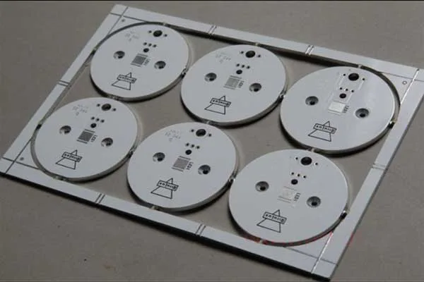
We are a manufacturer specializing in the production of multilayer metal core PCBs, which are designed to dissipate heat efficiently and reliably for high-performance electronic applications.
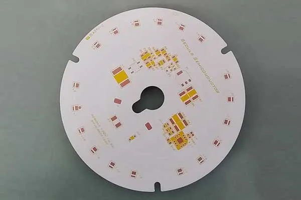
We offer a comprehensive multilayer aluminum PCB fabrication service that is tailored to meet the needs of our customers in various industries, such as automotive, aerospace, and LED lighting.
JHYPCB offers high-quality multilayer PCB manufacturing services up to 64 layers, utilizing advanced production equipment and a strict quality control system to ensure precision and efficiency for every project.
Our Multilayer PCB Prototyping Service provides high-quality and reliable printed circuit boards that are designed and fabricated to meet the exact specifications of our clients. With our advanced manufacturing capabilities and expertise in the industry, we offer fast turnaround times and affordable prices for multilayer PCBs ranging from 2 to 10 layers.
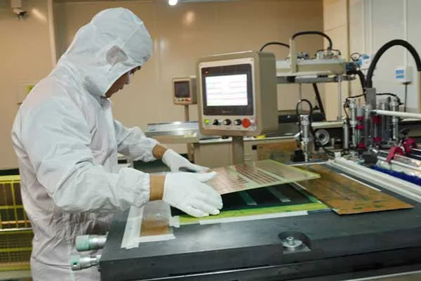
Our state-of-the-art equipment and skilled technicians ensure that each PCB we produce meets the highest standards for quality and performance. We use advanced software for designing the PCB layouts, and our production processes are optimized for accuracy and efficiency. We also conduct rigorous testing and quality control checks to ensure that every PCB we deliver is free of defects and fully functional.
In addition to our standard multilayer PCB prototyping service, we also offer customization options such as different substrate materials, surface finishes, solder masks, and silkscreen printing. We work closely with our clients to understand their specific requirements and offer personalized solutions to meet their unique needs.
A multilayer PCB is a printed circuit board that has more than two layers of conductive material separated by insulation material. These layers are interconnected by vias that allow electrical signals to pass between the layers.
Multilayer PCBs offer several advantages over single or double-sided PCBs, including higher circuit density, better signal integrity, and reduced electromagnetic interference (EMI).
There is no fixed minimum number of layers for a multilayer PCB. However, most multilayer PCBs typically have at least four layers.
Multilayer PCBs are manufactured using a process called lamination. This involves bonding together multiple layers of copper-clad PCB material with a layer of insulating material in between. The layers are then drilled and plated to create the required circuit patterns.
Blind vias are vias that connect an outer layer of the PCB to an inner layer without passing through the entire board. Buried vias are vias that connect two or more inner layers of the PCB without passing through the outer layers.
Design considerations for multilayer PCBs include proper layer stackup, via placement, and power and ground planes to minimize EMI and signal integrity issues.
A power plane is a layer in a multilayer PCB that is dedicated to carrying power to the various components on the board. It is typically placed adjacent to a ground plane to reduce EMI and improve signal integrity.
A ground plane is a layer in a multilayer PCB that is dedicated to providing a low-impedance ground connection to the various components on the board. It is typically placed adjacent to a power plane to reduce EMI and improve signal integrity.
In a symmetrical layer stackup, the layers are arranged symmetrically around the center layer of the PCB. This results in more uniform electrical characteristics and can be beneficial for high-speed digital applications. In an asymmetrical layer stackup, the layers are arranged asymmetrically around the center layer, which can be more space-efficient but may result in more complex signal routing.
When you partner with us, we do everything to ensure your PCB manufacturing and assembly are completed on time to your specifications with the highest quality.
Fill out the form below, and we will get back to you within the next 24
hours to complete the order, and then you’re all set to get started!