
What is HDI PCB Stackup – Different Stackups for HDI PCBs
In this article, we will discuss the different types of
Leading manufacturer of PCB Fabrication and Assembly in China.
In today's world of advanced technology, high-density interconnect (HDI) printed circuit boards (PCBs) are playing an increasingly vital role in the development of compact, high-performance electronic devices. With the rapid advancement of technology, the demand for smaller, lighter, and more powerful electronic devices is growing at an unprecedented rate. HDI PCBs are becoming increasingly popular due to their ability to pack more components into a smaller area, resulting in more efficient, cost-effective, and reliable devices. At JHYPCB, we are your trusted PCB manufacturer in China, offering rapid PCB prototyping, quick turn PCB fabrication, HDI PCB prototype and mass production service.
JHYPCB
HDI PCBs were first developed in the 1980s, as the demand for smaller and more powerful electronic devices grew. Traditional PCBs with through-hole components were limited in their ability to accommodate small and densely packed components. HDI PCBs addressed this limitation by using blind and buried vias to create a more compact and efficient design.

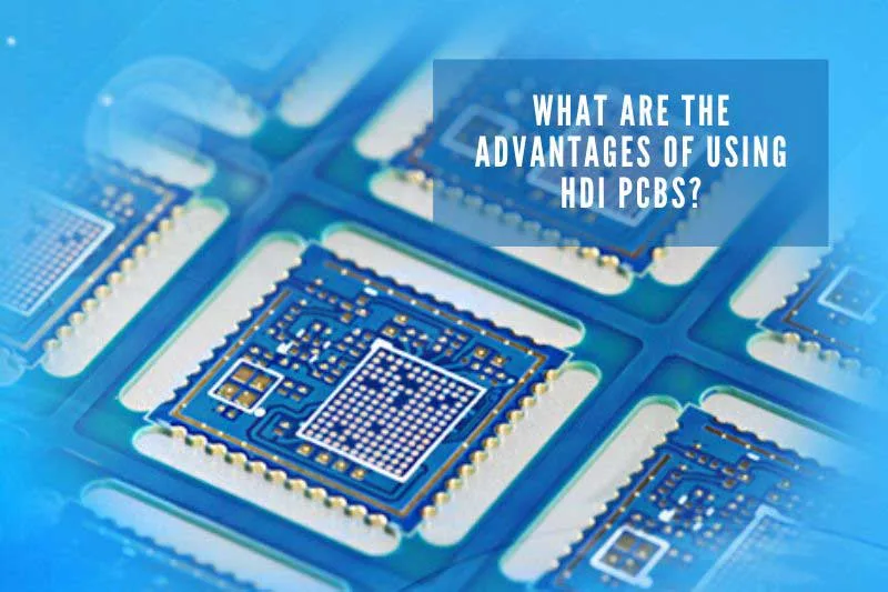
HDI PCBs are used in a wide range of electronic devices, including smartphones, tablets, laptops, medical equipment, and aerospace systems. They offer several advantages over traditional PCBs, including:
HDI PCBs have a wide range of applications in various industries due to their advanced features and benefits. Some of the common applications of HDI PCBs are:
HDI PCBs come in several different types, each with its own unique characteristics and design considerations. The following are some common types of HDI PCBs:


Stacked and Non-Stacked HDI PCBs are two different high-density interconnect PCB designs, which differ primarily in the number of internal connection layers.
Non-Stacked HDI PCBs feature a single substrate connected by multiple layers or blind/buried vias to achieve higher circuit density. This design typically uses one or two internal layers, each containing blind or through vias to route signals between different layers.
Stacked HDI PCBs achieve even higher circuit density by stacking multiple internal layers on a single substrate. Signal transmission across multiple internal layers is achieved through interweaving vias, either blind or through, between different layers. Stacked designs can achieve very high circuit densities, but require more complex manufacturing and design techniques.
The manufacturing process of HDI PCBs involves several complex steps, including layer stacking, drilling, copper plating, photoresist coating and exposure, metalization, controlled depth back drilling, punching, routing and milling, solder mask and silkscreen printing, and surface finishing. Each step must be carefully controlled and monitored to ensure the quality and reliability of the finished product.
As a professional PCB manufacturer, our HDI PCB manufacturing capabilities are always advancing to meet the ever-growing demands of modern electronic devices. Thanks to advanced technologies such as laser drilling and high-density interconnects, we can now produce HDI PCBs with smaller form factors, faster transmission speeds, and more integrated functionality. We understand the importance of quality control and testing in the HDI PCB manufacturing process to ensure reliable and stable performance. With our expertise and commitment to excellence, we can provide you with high-quality HDI PCBs that meet your specific needs and exceed your expectations.
| Manufacturing Capability | Specification |
|---|---|
| Layer Count | 2-40 layers |
| Minimum Line/Space | 25/25 µm (1/1 mil) |
| Minimum Mechanical Drill | 0.1 mm (4 mil) |
| Minimum Laser Drill | 0.075 mm (3 mil) |
| Aspect Ratio (Mechanical) | 10:1 |
| Aspect Ratio (Laser) | 1:1 |
| Maximum Panel Size | 610 mm x 610 mm (24″ x 24″) |
| Maximum Copper Thickness | 10 oz |
| Minimum Copper Thickness | 9 µm (0.5 oz) |
| Minimum Finished Hole Size | 0.15 mm (6 mil) |
| Maximum Plated Hole Size | 0.4 mm (16 mil) |
| Minimum Solder Mask Bridge | 0.05 mm (2 mil) |
| Minimum SMT Pitch | 0.3 mm (12 mil) |
| Surface Finish | ENIG, OSP, HASL, Immersion Tin, Immersion Silver, ENEPIG |
| Quality Standards | IPC Class II and Class III, ISO 9001, UL, RoHS |
| Testing | Electrical Testing, Flying Probe Testing, AOI, X-ray Inspection |
Quality assurance and testing for HDI PCBs involve using methods such as optical and X-ray inspection, probe testing, and electrical testing to detect defects and verify the performance of the PCB. Strict quality control procedures and adherence to standards such as IPC-6012 and IPC-6013 are also essential to ensure that the finished product meets the required specifications.
HDI PCB design requires careful consideration of trace width and spacing, via placement and size, ground and power planes, high-speed signal transmission and control, and reflection and crosstalk. Designers need to balance these factors to ensure that the finished product meets the desired performance and reliability requirements.
Here are some possible trends and developments that can be expected for HDI PCBs in the future based on the demands and challenges of various industries:
Are you in need of high-quality HDI PCB manufacturing services for your electronic devices? Look no further than our professional PCB manufacturing company. With years of experience and expertise in HDI PCB manufacturing, we are dedicated to providing you with the best possible solutions to meet your specific requirements. Our state-of-the-art facilities and advanced technologies enable us to produce HDI PCBs with high-density interconnects, faster transmission speeds, and more integrated functionality. Our commitment to quality control and testing ensures that every HDI PCB we produce is reliable and stable, meeting the highest industry standards. Contact us today to learn more about our HDI PCB manufacturing capabilities and how we can help you bring your electronic devices to the next level.

In this article, we will discuss the different types of

In HDI PCB design, three types of holes are commonly

HDI PCBs and traditional PCBs offer different advantages and disadvantages,
In the relentless pursuit of smaller, faster, and more powerful

This article will discuss some key considerations for choosing an
When you partner with us, we do everything to ensure your PCB manufacturing and assembly are completed on time to your specifications with the highest quality.
Fill out the form below, and we will get back to you within the next 24
hours to complete the order, and then you’re all set to get started!


