PCB Manufacturing Services

The Ultimate Guide to Double Sided PCBs

JHYPCB is a professional PCB manufacturer based in China, specializing in providing high-quality double-sided PCB fabrication and assembly services to customers worldwide. With over 10 years of experience in the PCB industry, we have the expertise and capabilities to manufacture complex double-layer boards cost-effectively.

At JHYPCB, we utilize cutting-edge equipment and technologies to produce premium double-sided PCBs. Our SMT lines can assemble components as small as 0201 chips and BGAs, meeting the needs of miniaturization. And we adopt strict quality control methods like AOI inspection to ensure each board meets your specifications perfectly.

Our double-sided PCB fabrication process leverages precision lithography, etching, drilling, and plating technologies to create intricate circuit patterns on both sides of the board, connected by plated through holes. We can manufacture multilayer PCB boards with 4-64 conductive layers, blind/buried vias, and other features for your application.

Whether you need prototype double-sided PCBs in small batches or mass production runs, JHYPCB has the capabilities to fulfill your requirements. Our efficient operations allow us to offer rapid turnaround times, often shipping orders within just 48 hours. When you choose us for your double-layered PCB needs, you can expect nothing less than superb quality and service.

Contact our engineering team today to get a free quote for your custom double-sided PCB design. We are committed to providing the most suitable solution that fits your technical specifications and budget needs.

Benefits of Choosing JHYPCB for Double Sided PCBs

JHYPCB offers you a number of advantages when you choose us for your double sided PCB requirements:

Cost-Effective Pricing

Our large production capabilities and efficient operations allow us to provide very affordable pricing for double sided PCBs, without compromising on quality. We offer price incentives on larger order quantities.

Fast Turnaround Time

Our streamlined manufacturing process reduces production time to get your double layered PCBs delivered faster. We provide among the fastest turnaround times in the industry, as fast as 48 hours for prototype orders.

Rigorous Quality Control

We perform extensive inspection and testing at every stage of double sided PCB fabrication, including AOI, flying probe testing, etc. This stringent quality control ensures your boards are defect-free.

One-Stop Service

We offer both PCB fabrication and component assembly for double sided boards under one roof. This simplifies procurement and enables better quality control and turnaround time.

Excellent Customer Service

Our engineering team provides exceptional technical assistance and support for your double sided PCB orders. You can expect responsible service and expert guidance.

By choosing JHYPCB for your double layered PCB manufacturing needs, you get the combined benefits of affordable pricing, rapid delivery, robust quality, convenient one-stop service, and reliable customer support. Contact us today to get started on your project!

What is a Double Sided PCB?

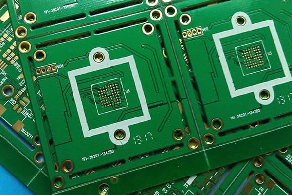
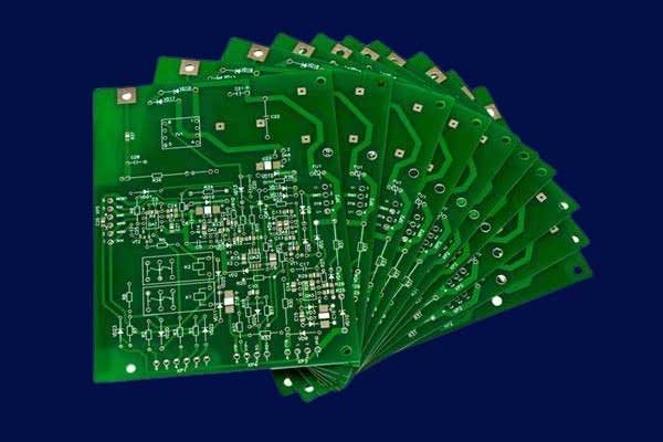
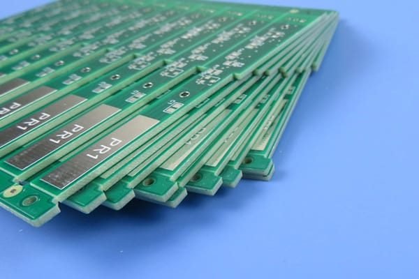
A double-sided printed circuit board has conductive copper tracks etched on both the top and bottom surfaces. Components are mounted and soldered onto the tracks on both sides. The two sides are connected by plated through holes called vias. This allows greater component density and more complex circuit designs.

Double-sided PCBs are commonly used in products like electronics, telecommunications devices, industrial control units, medical equipment, aerospace avionics, and more. The key advantages are reduced size and increased functionality.

Double Sided PCB Stack up

Get a Double Sided PCB Quote

JHYPCB's Double Sided PCB Fabrication Process

At JHYPCB, we use advanced manufacturing technologies and techniques to fabricate high-quality double-sided PCBs:

  • We start with a dielectric substrate material like FR-4 and use precision lithography to transfer the circuit pattern onto both sides.
  • Next, chemical etching removes unwanted copper to leave behind the desired tracks.
  • Drilling forms the holes and vias, which are then plated with copper to form connections between layers.
  • A solder mask is applied to protect the copper traces, while exposing pads.
  • Silkscreen printing labels components placements and identifications.
  • Finally, a protective finish like ENIG, HASL/Lead-free HASLImmersion Tin, or OSP is added.

We perform extensive testing and inspection after each process stage to ensure perfect layer-to-layer registration and reliable plated through-hole connections on the finished boards.

JHYPCB´s technical specification and Capabilities

Feature Capability
Number of Layers 2 Layers
Technology highlights Epoxy glass dielectric materials laminated with copper cladding of varying thicknesses.
Materials FR-4 standard, FR-4 high performance, Aluminium, High Tg, Halogen-free, Rogers, Teflon, ISOLA
Min. Trace Width and Space 0.075mm/0.065mm
Min.Hole Size 0.1mm
Min.Blind/Buried Via 0.1mm
Surface Finish Lead-Free HASL, OSP, ENIG, Immersion Silver, Immersion Tin, Gold Plating, ENIG+OSP
Max.Board Size 2000mm*610mm

Get a Custom Quote for Your Double Sided PCBs from JHYPCB:

Getting an instant quote at JHYPCB for your custom double-sided PCBs is quick and easy:

  1. Upload Gerber Files and BOM via Online Form

You can upload your design Gerber files and BOM through our online form. This allows our engineers to review your detailed design specifications.

  1. Send Your Specific Requirements via Email

Alternatively, you can email your specific fabrication requirements directly to sales@pcbjhy.com. Provide details like PCB dimensions, layer count, material, quantities, lead time, and any special manufacturing specs.

  1. Receive a Customized Quote

Our sales team will provide you with a customized quote for your double-sided PCBs based on the information you provide. The quote will contain a complete cost breakdown.

  1. Place Order and Get Manufacturing and Delivery

If our quote satisfies your needs, you can directly place an order via email. We will start production immediately upon receiving your order, and deliver the double sided PCBs within the agreed lead time.

By contacting our sales team directly, you can quickly get a customized quote for JHYPCB’s double sided PCB fabrication. Email us now to get started on your project!

Get a Double Sided PCB Quote

Conclusion

In conclusion, double-sided PCBs are an essential component of modern electronics, offering a high level of functionality and reliability. As the demand for smaller, more complex devices continues to grow, the development of advanced PCB fabrication and assembly techniques will be essential to meeting the challenges of this rapidly evolving industry. We must continue to push the boundaries of what is possible and invest in new technologies to ensure that the electronic devices of the future are both efficient and sustainable.

If you are looking for a reliable PCB manufacturer that can offer both double-sided PCB prototypes and mass production, look no further. Contact us today to discuss your specific needs and find out how we can help you take your projects to the next level. Thank you for considering us as your partner in PCB manufacturing.

Double Sided PCB FAQs

The most commonly used materials for double-sided PCBs are FR-4 (a type of fiberglass epoxy) and polyimide (a high-temperature plastic).

A double-sided PCB has circuits and components on both sides of the board, while a multi-layer PCB has multiple layers of circuitry separated by insulating material.

The copper thickness used for double-sided PCBs can vary depending on the application, but the most common thicknesses are 1 oz, 2 oz, and 3 oz.

Through-hole components have leads that go through holes in the PCB and are soldered on the other side, while surface mount components are mounted directly onto the surface of the PCB.

Yes, double-sided PCBs can be designed for high-frequency applications, but special attention needs to be paid to the placement of components and routing of traces to minimize interference.

The maximum size of a double-sided PCB is limited by the manufacturing process and the size of the materials used. Generally, double-sided PCBs can be made up to several feet in size, but larger sizes may require a different manufacturing process.

Yes, double-sided PCBs can be made for prototyping and low-volume production. Many PCB manufacturers offer prototyping and small-batch services for double-sided PCBs.

Vias are used to connect circuits on both sides of the PCB. They are drilled through the board and lined with conductive material, allowing current to flow between the layers.

Blind vias connect one or more inner layers of the PCB to one or both outer layers, while through vias connect all layers of the PCB.

Solder mask is a protective layer applied to the surface of the PCB to prevent solder from flowing where it's not supposed to. Silkscreen is a layer of ink applied to the surface of the PCB to identify components and provide additional information.

The most common types of surface finish used in double-sided PCBs are electroless nickel immersion gold (ENIG), immersion silver, HASL Lead Free, and organic solderability preservative (OSP).

The lead time for a double-sided PCB order can vary depending on the manufacturer and the complexity of the design, but typical lead times range from several days to several weeks.

The cost of a double-sided PCB depends on the size, complexity, and quantity of the order, as well as the type of materials and manufacturing processes used. Generally, double-sided PCBs are more expensive than single-sided PCBs but less expensive than multi-layer PCBs.

When choosing a PCB manufacturer for your double-sided PCB, consider factors such as experience, certifications, capabilities, lead times, and customer service. It's also important to ask for references and samples of previous work.

Double-sided PCBs can be repaired, but the process can be more challenging than repairing a single-sided PCB. Repairing a double-sided PCB may require removing components, drilling new holes, and re-routing traces, among other tasks. It's often more cost-effective to replace a damaged double-sided PCB rather than attempting to repair it.

Related Reading

Scroll to Top

Request A Quote

Let’s Do This!

Fill out the form below, and we will get back to you within the next 24
hours to complete the order, and then you’re all set to get started!