


Your Trusted Prototype PCB Manufacturing And Assembly Partner.
When you partner with us, we do everything to ensure your PCB manufacturing and assembly are completed on time to your specifications with the highest quality.
Leading manufacturer of PCB Fabrication and Assembly in China.
Welcome to JHYPCB’s comprehensive guide on PCB drilling. JHYPCB is a leading PCB manufacturer based in China, with over a decade of expertise in the industry. We specialize in providing high-quality PCBs to clients worldwide, and our commitment to quality and customer satisfaction has made us a trusted name in the industry.
Drilling is a fundamental step in the PCB manufacturing process and plays a crucial role in ensuring the functionality and reliability of the final product. A properly drilled PCB allows for the proper placement of components and connections, ensuring that the electrical signals pass through the board without interference. At JHYPCB, we understand the importance of drilling in PCB manufacturing, and we have invested heavily in the latest drilling equipment and techniques to ensure that our clients receive the best quality PCBs.
This guide will provide a comprehensive overview of PCB drilling, including drilling principles, equipment, and techniques, commonly faced challenges, and quality control measures. By the end of this guide, you will have a thorough understanding of the PCB drilling process and its importance in PCB manufacturing. So, let’s dive in!
PCB drilling is a critical process in the manufacturing of printed circuit boards. The purpose of PCB drilling is to create holes in the PCB that will later be used for mounting electronic components. These holes, also known as vias, provide the necessary electrical connections between different layers of the PCB.
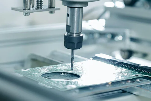
The PCB drilling process involves the use of a drill to create the required holes in the PCB. The drill is typically operated by a computer-controlled machine called a CNC (Computer Numerical Control) drilling machine. The drill bits used in PCB drilling are typically made of tungsten carbide, which is a hard and durable material that can withstand the high temperatures and pressures generated during drilling.
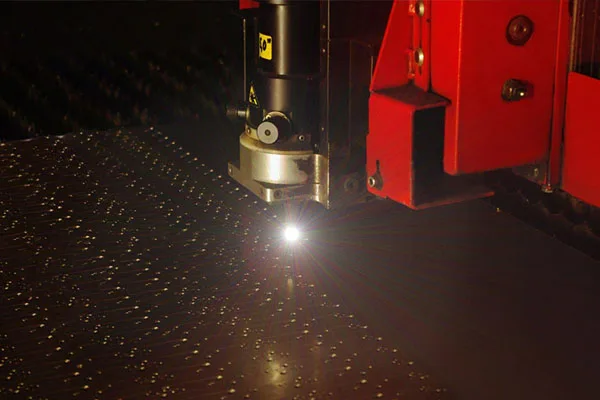
There are several different types of drills used in PCB drilling, including twist drills, diamond drills, and laser drills. Twist drills are the most commonly used type of drill and are suitable for drilling through most types of PCB materials. Diamond drills are used for drilling through hard materials like ceramics or glass, while laser drills are used for drilling extremely small holes that are too small to be drilled with other types of drills.
Precision and accuracy are crucial in PCB drilling because even small errors or deviations from the specified dimensions can result in faulty PCBs that may not function properly. The drilling process must be carefully controlled to ensure that each hole is drilled to the correct depth, diameter, and position on the PCB. For this reason, modern PCB drilling machines are equipped with advanced features like automatic tool changers, high-speed spindles, and computer vision systems to ensure precise and accurate drilling.
PCB manufacturing requires the use of drilling machines to create holes for component placement and connectivity. There are different types of drilling machines used in PCB manufacturing, including vertical drilling machines and horizontal drilling machines. Vertical drilling machines are typically used for single-sided and double-sided PCBs, while horizontal drilling machines are used for multilayer PCBs.
Aside from the drilling machines themselves, there are also different types of drilling technologies used in PCB manufacturing. The most common drilling technologies include mechanical drilling and laser drilling. Mechanical drilling is the most widely used technology and relies on rotating bits to create holes in the PCB. Laser drilling uses high-powered lasers to create small precision holes.
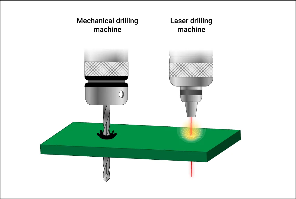
Mechanical and laser drilling comparison
The choice of drilling technology depends on the type of PCB being manufactured and the level of precision required. For example, mechanical drilling is suitable for most standard PCBs, while laser drilling is used for high-density interconnect (HDI) PCBs that require small and precise holes.
Using advanced drilling equipment and technology offers several benefits in PCB manufacturing. Firstly, advanced drilling equipment and technology can produce more precise and accurate holes, resulting in improved PCB performance and reliability. Secondly, advanced drilling equipment and technology can improve manufacturing efficiency by reducing lead times and minimizing the need for additional processes such as hole plating. Finally, using advanced drilling equipment and technology can improve overall product quality while reducing costs in the long run.
PCB manufacturing involves two vital processes: PCB drilling and through-hole plating. During drilling, holes or slots are created on the circuit board, which are used for securing components and interconnecting different layers. To establish electrical connections, the drilled structures must be plated with copper to enable conductivity. This process is known as through-plating or via plating.
The drilling process begins after the lamination process is complete and is followed by hole plating. The following flowchart illustrates the order in which these processes occur:

One approach to categorizing PCB drill holes is based on their conductive properties, which fail to fully capture the importance of drill holes in circuit board structures. A more comprehensive method of classifying and differentiating drill holes is based on their specific applications, as detailed below.
PCB Drill Hole Types:
2. Non-Plated Through Holes

| Drill Hole Type | Automated CNC Drilling | Mill Machine | Laser Drilling |
|---|---|---|---|
| Press-fit | Yes | Yes | No |
| Mounting hole | Yes | Yes | No |
| Countersink (back drilling) | Yes | Yes | No |
| Through-hole | Yes | Yes | No |
| Blind Via | Yes | Yes | No |
| Buried Via | Yes | Yes | No |
| Microvia | No | No | Yes |
| Thermal via | Yes | Yes | No |
| Feature | Tolerance |
|---|---|
| Drill tolerance for PTH | ±3 mils |
| Drill tolerance for NPTH | ±2 mils |
| Via location | 1 mil |
Drilling is a multi-faceted process that involves much more than simply creating holes of specific dimensions. The overall efficiency of the process is determined by a variety of factors, including those outlined below.
Aspect Ratio
The aspect ratio (AR) for a through-hole is defined as the ratio of the hole’s length to its diameter. It is an important consideration in PCB manufacturing because it affects the plating process. A higher AR value means that the through-hole is deeper and narrower, which can lead to difficulties in the plating process. This is because the plating solution must travel a longer distance to coat the entire interior surface of the hole. The solution may also struggle to fill the hole completely, resulting in poor plating quality.
The thickness/depth of the microvias is not the same as that of the board. Hence for microvias, the aspect ratio is defined as the ratio between the depth of the ]hole and its diameter.
For through-holes, the ideal aspect ratio is 10:1 and for microvias, it is 0.75:1.
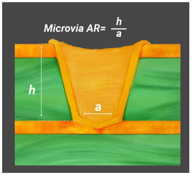
Aspect ratio (AR) for a through-hole
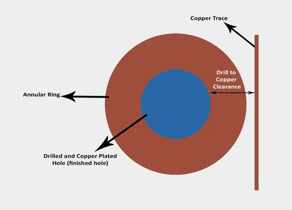
Annular ring and drill-to-copper
An annular ring is the area on a PCB around a drilled hole that remains after the hole has been drilled and plated. It is the measurement from the edge of the hole to the edge of the copper pad on the surface layer of the PCB. The size of the annular ring is important for proper functionality of the circuit, and it is affected by a number of factors, including the drill bit size, drill tool accuracy, and the intended current carrying capacity of the trace.
Drill-to-copper is the length of the conductive path between the surface of the PCB and the inner layers, as determined by the drill depth. It is an important consideration in the design of PCBs, as it affects the overall thickness of the board and can also impact the manufacturing processes used to create the board. The drill-to-copper measurement is typically specified in the design files for the PCB and is carefully controlled during the manufacturing process to ensure the board functions as intended.
The finished hole to copper clearance will be the drill to copper clearance along with the copper plating thickness. Finished hole to copper clearance = drill to copper clearance + plating thickness x 2.
If the drill diameter is 6 mil and the plating thickness is 1 mil, then: finished hole to copper clearance = 6 + 1 x 2 = 8 mil.
Annular ring and drill-to-copper
There are several challenges that arise during the PCB drilling process that can potentially impact the quality of PCB products. Here are four common challenges in PCB drilling:
Any of these challenges can have negative effects on the quality of the final PCB product. They can lead to scrapped PCBs, decreased conductivity, and other problems that can affect product functionality and reliability. Therefore, it is important to take measures to prevent these issues and ensure a high-quality finished product.
Quality control and inspection are critical aspects of the PCB drilling process because they ensure the final product meets both the design specifications and the requirements of the end-user. PCB drilling involves drilling holes of various types such as through-holes, blind vias, buried vias, and micro-vias. The holes must be drilled accurately and in the correct location to ensure proper connections between the different layers of the PCB.
Quality control and inspection can help prevent issues such as drill bit breakage, drill wandering, dust and debris, burrs and rough edges, and drill bit wear. To ensure quality and accuracy, various testing methods are used during the drilling process, including:
In summary, quality control and inspection are crucial to ensuring the accuracy, reliability, and safety of PCB products. Various testing methods are used to verify the quality and accuracy of the drilled holes, ensuring that a high-quality PCB is delivered to the end-user.
To ensure high-quality PCB drilling process, it is necessary to check the following:
What is through-hole plating?
Through-holes refer to holes that are drilled through the entire depth of a circuit board, starting from the top layer and ending at the bottom layer. These holes are plated with copper in a process known as through-plating, which makes them electrically conductive. Non-plated through-holes (NPTH) are not meant to provide electrical conduction and therefore, do not require plating.
For through-plating, we generally aim for a thickness between 0.0008″ to 0.0012″ (20 to 30 microns). The maximum hole size permitted for plated holes is 246 mils.
Two techniques are available for plating, namely electroless copper plating, and electroplating.
The through-hole plating process generally involves the use of electroless copper plating, which deposits a uniform layer of copper on the targeted area. The process involves several steps, including cleaning the bare boards in a series of baths, covering the required coating areas with a catalyst such as Palladium, and then immersing them in a copper salt and reducing agent bath such as formaldehyde. This results in copper deposition on the inner surface of the hole region.
However, the copper plating of the interior part of the holes can be challenging when the hole diameter is small while the depth is significant, i.e., a high aspect ratio. In such cases, a copper plating bath with high throwing power is necessary to allow the solution to penetrate the tiny and deep holes and deposit copper inside them. The high throwing power allows the copper ions to reach the bottom of the holes instead of depositing only on the surface, ensuring uniform copper coverage throughout the hole. This is critical since uneven copper plating thickness can lead to short circuits or open circuits and ultimately hinder the PCB’s overall performance.
In the electroplating process, an anode, cathode, and electrolyte are used. The application of electricity initiates conduction to initiate the plating process. This method is generally suitable for plating the surfaces of PCBs and not for through-holes.
Drilling and through-hole plating require utmost care and precision as these expensive processes determine the overall cost and efficiency of the PCB. Different through-plating processes require different electroplating methods to ensure uniformity and quality in plating. For instance, small through-holes with a depth-to-diameter ratio less than one require the use of high-tensile copper electroplating solution to ensure uniform plating. These requirements call for highly skilled technicians to perform meticulous operations and inspections.
The aspect ratio of a PCB hole is calculated by dividing the depth of the hole by its diameter.
Aspect ratio (AR) = (Depth of the hole/ Diameter of the drilled hole)
For example, if a hole is 1.5 mm in diameter and 3 mm deep, the aspect ratio would be 2:1. It is important to consider the aspect ratio when designing the PCB, because it can affect the plating process of the hole during fabrication. If the aspect ratio is too high, it can be difficult to ensure proper plating of the hole, and this can lead to issues with connectivity.
Drilling is used to create holes in the PCB to accommodate components, interconnects, and vias. These holes are then plated with copper to create electrical connections between layers of the PCB.
PCB drilling is a critical step in printed circuit board (PCB) manufacturing. It creates the holes that allow different components to be mounted and connected on the board. Proper drilling ensures:
So in summary, accurate PCB drilling makes sure components are securely mounted and properly connected, which enables the board to work correctly. It is a crucial fabrication step that requires precision and care.
PCB drills typically use tungsten carbide or diamond-tipped drill bits to create precise holes. These drills are usually very small, with diameters ranging from 0.1mm to 6mm.
The drilling must be very precise, with tolerances typically in the range of 0.025mm to 0.1mm. This is necessary to ensure that the components fit properly and that the electrical connections are reliable.
The PCB is first drilled with a pilot hole to guide the larger drill bit. The larger bit is then used to create the final hole, which is typically plated with copper to create an electrical connection.
Through-hole vias run all the way through the PCB, while blind vias only go partway through the PCB. Blind vias are used when space is limited and only need to connect a few layers of the PCB.
PCB drilling can be a costly and time-consuming process, especially for boards with many layers or small vias. The cost of drilling is directly related to the complexity of the board, and it can significantly affect the overall cost of PCB production. Accurate drilling requires skilled operators and high-quality equipment, which can also affect efficiency.
The working principle of a PCB CNC drilling machine is to control the position and depth of the drill bit through a CNC system in order to perform drilling operations. The CNC system can automatically control the movement and stopping of the drill bit according to a pre-set program, thus achieving efficient and precise drilling operations. During the drilling process, the CNC system can also monitor the status of the drill bit, such as the degree of wear and tear, drilling depth, etc., in order to adjust the position and depth of the drill bit in a timely manner, ensuring the quality and accuracy of the drilling.
The main difference between laser drilling and mechanical drilling is the way in which the hole is created. In mechanical drilling, a rotating drill bit physically removes material from the PCB substrate to create the hole. In contrast, laser drilling uses a high-energy laser beam to melt and vaporize the material, creating a hole without any physical contact with the substrate.
Mechanical drilling is typically used for creating larger holes (>0.25mm) and is a relatively straightforward and cost-effective process. Laser drilling, on the other hand, is better suited for creating smaller holes (<0.25mm) that require higher precision and accuracy. It can be more expensive due to the need for specialized equipment and the higher cost of laser maintenance and operation.
The choice between mechanical and laser drilling depends on the specific requirements of the PCB design. If the design includes small or complexly shaped holes, laser drilling may be the better option. However, for larger holes or simpler designs, mechanical drilling may be more appropriate.
Yes, it is possible to drill holes on a flexible printed circuit board (PCB), but the drilling process for flexible PCB is different from that of rigid PCB due to the unique characteristics of flexible materials. Specialized equipment, such as laser drills or routers, may be used to drill holes on flexible PCBs. The process also requires careful consideration of the drilling angle, speed, and pressure to prevent damage to the flexible material.
Screw holes on a PCB are used to securely attach the PCB to a chassis or other mechanical components. These holes are typically drilled in the PCB during the manufacturing process and are usually threaded so that screws can be directly inserted into them. The location, size, and number of screw holes depend on the specific application and the mechanical requirements of the PCB. It is important to ensure that the screw holes are positioned away from any critical signal traces or components that may be sensitive to mechanical stress.
PCB drilling is necessary for creating the holes that will eventually become the electrical connections between different layers of the PCB, or to connect the PCB with other components. Holes are also needed for mounting components and for through-hole or surface-mounting technology. Additionally, PCB drilling is necessary for creating space for vias, which are the conduits that enable electrical connections between layers of the PCB.
The best drill bit for PCB drilling is typically a solid carbide drill bit. Carbide is a hard, durable material that maintains its sharp edge and resists wear over time, such as Tungsten Carbide micro drill bits. It is also more resistant to heat than other types of materials, which is important since drilling PCBs can generate a lot of heat. Solid carbide PCB drill bits are also available in a variety of diameters to accommodate different size holes needed for the PCB design.
PCB drilling techniques have improved greatly to meet the needs of modern electronics. Key trends include:
CNC (Computer Numerically Controlled) machines are automated drilling machines that are essential for modern PCB (printed circuit board) fabrication. They utilize advanced computer control to deliver unmatched precision, speed and consistency in the PCB drilling process.
Modern CNC drilling machines now include advanced software, multi-spindle drills, lasers, precision linear motors, in-process inspection and more. These innovations enable them to drill denser boards faster while maintaining exceptional quality standards. Leading CNC makers continue improving them to meet the needs of evolving PCB designs.
While manual drilling is still used in some applications, CNC machines are overwhelmingly favored for medium to high-volume PCB production. The precision and efficiency they provide are unmatched. For prototype runs, manual mills or low-end machines may suffice but CNC remains the gold standard for professional PCB drilling.
When you partner with us, we do everything to ensure your PCB manufacturing and assembly are completed on time to your specifications with the highest quality.
Fill out the form below, and we will get back to you within the next 24
hours to complete the order, and then you’re all set to get started!