


Your Trusted Prototype PCB Manufacturing And Assembly Partner.
When you partner with us, we do everything to ensure your PCB manufacturing and assembly are completed on time to your specifications with the highest quality.
Leading manufacturer of PCB Fabrication and Assembly in China.
Welcome to JHYPCB’s guide to back drilling in PCBs! If you’ve been involved in PCB design or manufacturing, you may have heard about this advanced technology that helps reduce signal interference and improve circuit performance. Back drilling involves selectively removing excess copper from the vias or through holes of multilayer PCBs, leaving only the necessary length to interconnect the adjacent layers. This process can be particularly useful in high-speed transmission lines, where signal integrity is critical. In this guide, we’ll explain in detail how back drilling works, its benefits, and some real-life examples of its applications. So, let’s dive in and explore the world of back drilling!
Back drilling, sometimes also called controlled-depth drilling or conductor back-etching, is a PCB manufacturing technique that involves removing the unused section of a via or through-hole using a specialized drilling process. The goal of back drilling is to eliminate or reduce the portion of the via that is not needed for electrical connectivity between the layers of the PCB. This excess copper or dielectric material, if left untouched, can act as an antenna that picks up unwanted noise or crosstalk from adjacent signals or power planes. By removing it, back drilling can significantly improve signal integrity and reduce interference, especially in high-speed designs.
The back drilling process happens after the through-holes are plated but before the final board fabrication steps. Typically, a dedicated router or drill is used to perform the drilling, which requires precise control over the depth and diameter of the removal. The exact drill bit size and cutting depth depend on the thickness and number of the board layers, as well as the desired impedance and signal rise/fall time. Multiple back drill operations may sometimes be needed to achieve the desired results.
It’s worth noting that back drilling is not a new technique, and has been used in PCB manufacturing for several decades. However, its popularity has increased in recent years due to the rising demand for high-speed and high-density designs, as well as the availability of more advanced back drill equipment and software.
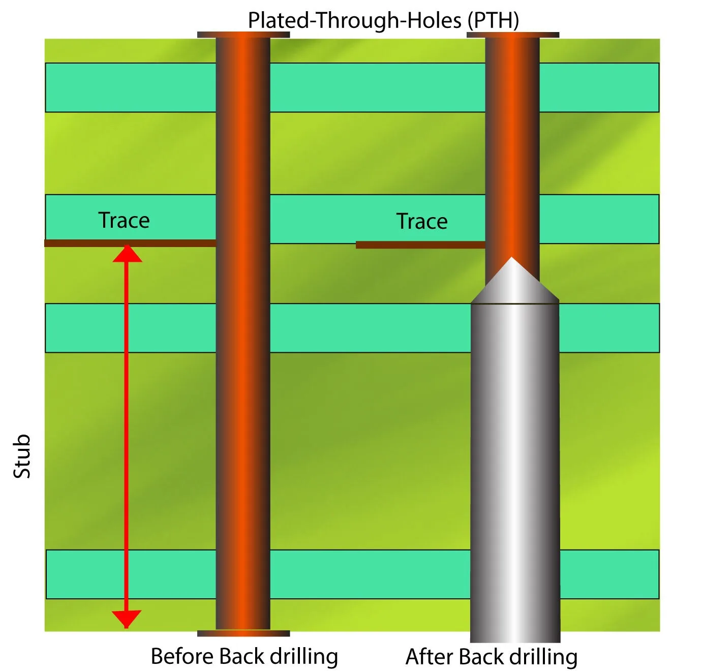
Back drilling is a technique that is used to create clean and precise holes in a printed circuit board that have already been drilled. The process involves drilling out the length of the vias or the through-holes from the opposite side of the board. This technique is widely used in modern PCBs for the purpose of reducing signal reflections and improving the performance of high-speed digital circuits.
The process of back drilling involves using specialized equipment to drill out the unwanted portion of the via or through-hole on the opposite side of the board. This is typically done using a CNC machine with a spindle and a special drill bit. The drill bit is designed to remove material from only the unwanted portion of the hole, leaving the desired portion untouched and intact.
One of the most commonly used back drilling techniques is called blind via back drilling, which involves drilling out the unwanted portion of a blind via from the back side of the board, leaving the remaining part of the via intact. The second technique is called through-hole back drilling, which involves drilling out the unwanted portion of a through-hole from the back side of the board.
When planning to use back drilling in a PCB, there are several factors that need to be considered. One of the most important factors is the aspect ratio of the holes. The aspect ratio of a hole is the ratio of its length to its diameter. A high aspect ratio can make it difficult to achieve accurate and precise back drilling. Therefore, it’s important to ensure that the aspect ratio of the holes is within a reasonable range.
Another important factor is the type of material used for the PCB. Materials like FR-4, which are commonly used for PCBs, can cause problems during back drilling due to their high glass transition temperature. The high temperature can cause the drill bit to wear out faster and can also cause the material to melt or deform during the drilling process.
After back drilling is complete, it’s important to measure and test the results to ensure that the desired outcome has been achieved. Measurement is typically done using an impedance meter or a time domain reflectometer (TDR) to check the impedance of the circuit and identify any reflections that may be present. Testing is typically done using a high-speed digital signal generator and an oscilloscope to check the performance of the circuit and identify any issues that may be present.
Back drilling is essential to achieving optimal signal integrity and improving the overall performance of PCBs. The following are some of the key benefits of back drilling:
Reduction of signal reflection and interference: Back drilling is necessary to eliminate the stub created during via drilling, which can cause signal reflection, ringing and interference. By removing the stub, the signal can travel through the via hole without reflection and distortion, leading to better signal quality and reduced interference.
Improvement in signal integrity and reliability: Back drilling also ensures that the signal impedance is consistent throughout the trace, via and component layers, which enhances the board’s signal integrity and reliability. This is because it minimizes the impedance mismatch that often leads to signal distortion and loss.
Enhancement of PCB performance: Back drilling helps to increase the performance of the PCB as a whole. This is achieved by improving the tolerances of the trace routing and via placement, which reduces the likelihood of signal degradation and noise. As a result, the board can operate at higher frequencies and with greater accuracy, making it more suitable for high-speed digital applications.
A limitation of back drilling is that it is suitable solely for high-frequency boards operating within the range of 1GHz to 3GHz and that lack viable blind vias. Moreover, a unique method must be employed to prevent any damage to the traces and planes positioned adjacent to the hole in the backside of the board.
Back drilling is a crucial process in PCB manufacturing that enhances signal quality and reduces noise interference. The process involves drilling holes in the board to connect multiple layers and then drilling back through the board to remove portions of the via holes. This process is carried out after the initial drilling to ensure that the holes have appropriate diameters that are consistent with the board’s requirements.
Initially, after the holes are drilled and before plating, a dry film is applied to the board’s positioning holes to seal them from any plating. Once the dry film has been applied, the holes are plated with copper, creating a conductive pathway. Afterward, outer layer graphics are created before graphic plating is carried out. Before graphic plating, the positioning holes require a dry film sealing treatment. This ensures that the positioning holes will not be plated during the graphic plating process.
To perform back drilling, the positioning hole created in the initial drilling process is used for alignment, and a drill is employed to remove portions of electroplated holes that require this process. This is done to reduce reflection on signals that pass through multiple layers of the board. It helps to make sure that the signal quality is improved and any noise created during the transmission of the signal is reduced.
Once the back drilling process has been completed, it is important to wash the board thoroughly to get rid of any remaining drill chips present in the back drilling process. Inspection of the board is carried out to verify that it has been correctly done, and signal integrity has been enhanced. This is to ensure that the board’s performance is not compromised, and any faults are detected and corrected before it can be used.


Back drilling is a specialized technique, and it is not always necessary for all PCB designs. However, there are certain conditions and scenarios when it becomes necessary to use back drilling, which are discussed below:
High-speed designs: Back drilling is necessary when there are high-speed signals on the PCB. It reduces signal reflections and ringing by removing the portion of vias that are no longer needed after they have been drilled and plated. This reduces the stub length and improves signal quality.
Dense PCB designs: Back drilling is useful in cases where the PCB is densely populated with components and there is not enough space to place decoupling capacitors close to the IC pins. By using blind and buried vias, the capacitor can be placed on the opposite side of the PCB and connected through a via. Back drilling can remove the unused portion of the via to free up more space for other components.
Compliance with design specifications: Sometimes, back drilling is necessary to comply with design specifications. For instance, if a specification requires controlled impedance and a minimum stub length, back drilling can be used to meet these requirements.
Cost-effective solution: Back drilling is a cost-effective solution for certain types of PCBs. Instead of redesigning the entire board, back drilling can be used to fix signal integrity issues or reduce layer count.
Comparison with other techniques like stub removal:
Stub removal is another technique used to reduce signal reflections and ringing. However, it involves physically removing the portion of the via that is not needed after it has been plated. This process can be time-consuming and costly, especially for boards with a large number of vias.
In contrast, back drilling is a more efficient and cost-effective technique that removes the unwanted portion of the via through mechanical drilling. Back drilling is faster and easier to implement as it is performed after the board has been drilled and plated. Additionally, back drilling can be used for buried and blind vias, which cannot be easily removed with stub removal. Overall, back drilling is a superior technique to stub removal for most high-speed designs.
Back drilling is required in printed circuit board (PCB) design to reduce signal distortion and improve signal integrity.
A signal trace on a PCB consists of a signal line on the top layer with a reference plane (usually a ground plane) on the layer just below it. When the signal line terminates on a connector or a via that passes through the board to the ground plane, the portion of the signal line between the via and the reference plane is no longer needed and can cause signal reflection or crosstalk. This is because the signal line and the reference plane form a transmission line that has a characteristic impedance, and the sudden change in trace width at the termination point can cause impedance changes that reflect the signal back along the transmission line.
Back drilling involves removing the unused portion of the signal line that extends beyond the termination point to prevent any signal reflection or crosstalk. This is typically done by drilling a hole from the top layer down to the reference plane layer, and then using a milling tool to remove the unwanted portion of the trace.
By back drilling signal vias and reducing the length of signal traces on a PCB, signal distortion and crosstalk can be minimized, resulting in a higher quality and more reliable circuit design.
In order to achieve proper back drilling for a PCB, it is essential to provide the manufacturer with separate output files that contain the back-drill layers and specifications detailing which layers require corresponding back drilling. The diameter of the back drilling holes must be at least 0.2mm larger than that of the first drill holes. The distance between the back drilling hole and the trace should be 0.35mm for the first drill and 0.2mm for the back drilling. When designing the PCB stack-up, the dielectric thickness must be considered to prevent drilling into traces that should not be drilled. If drilling is required for a specific layer, the dielectric thickness between adjacent layers that do not require drilling and that specific layer should be at least 0.2mm.
Furthermore, to optimize the back drilling process, it is crucial to minimize the number of via stubs and avoid blind vias. Placing vias in less critical areas and maintaining a minimum distance between back drill holes and signal traces can also help prevent signal reflection and other issues. Keeping back drill hole diameters small is important to avoid damaging traces and planes laterally to the backboard hole. Additionally, considering back drilling during the initial design phase can help ensure that necessary measures are taken to optimize signal integrity and prevent problems during the manufacturing process.
Back drilling is termed as controlled depth drilling as the depth of these holes is predetermined and controlled during the drilling process.
10 mil
Some alternative techniques include the use of laser-drilled microvias (also known as blind and buried vias) and stack-up arrangements where traces are relocated to layers that are closer to the end of the via stub.
The depth of the hole, also known as the Z-axis depth.
Reaching stub lengths below 10 mil requires a higher level of precision from the drilling machine, which adds complexity. Additionally, it raises manufacturing costs, making it tough to reduce stub length. However, if the manufacturer uses the most recent drilling equipment, it's feasible to achieve stubs of 2 to 3 mils. Be sure to inquire with your manufacturer.
When you partner with us, we do everything to ensure your PCB manufacturing and assembly are completed on time to your specifications with the highest quality.
Fill out the form below, and we will get back to you within the next 24
hours to complete the order, and then you’re all set to get started!