


Your Trusted Prototype PCB Manufacturing And Assembly Partner.
When you partner with us, we do everything to ensure your PCB manufacturing and assembly are completed on time to your specifications with the highest quality.
Leading manufacturer of PCB Fabrication and Assembly in China.
The market for communication and networking equipment is becoming increasingly competitive, and as such, it’s important to ensure that your devices have high quality, performance, and reliability. Printed Circuit Board is the heart of any electronic device and a critical component in achieving these goals. The PCBs used in Telecommunications and Networking Equipment need to meet strict technical specifications to ensure optimal performance and reliability. As a professional PCB manufacturing and assembly service provider, JHYPCB is committed to delivering high-quality, high-reliability PCB solutions to help you gain a competitive edge in the market.

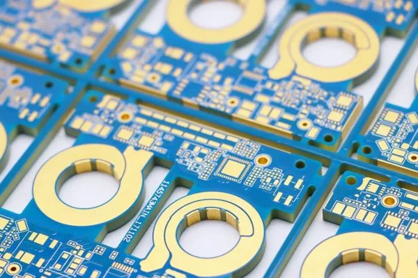
PCB, short for Printed Circuit Board, is a type of electronic board that connects and supports various electronic components mechanically and electrically. It is used in many electronic devices, including phones, computers, medical equipment, and of course, telecommunications and networking equipment.
PCBs are usually made of layers of copper traces and insulating material, such as fiberglass or resin, which provide the electrical connectivity and strength.
The manufacturing process of PCB typically involves several steps, including designing the layout of the circuit, printing the design onto the copper layer, etching the copper to form the circuit pattern, and drilling holes for components and connectors.
PCB technology has advanced significantly in recent years, enabling smaller and more complex designs with better performance and reliability.
Telecommunications and networking equipment refer to the devices and systems that facilitate communication and data exchange between different locations or networks. Some common examples include routers, switches, modems, wireless access points, base stations, and satellite receivers.
The demand for such equipment has been increasing rapidly due to the growing need for faster and more reliable connectivity in both personal and professional settings. The global telecommunications equipment market size was valued at USD 356.5 billion in 2020 and is expected to grow at a CAGR of 4.2% from 2021 to 2028.
With the constant advancement in technology and the increasing complexity of these devices, it is crucial to ensure that the PCBs used in telecommunications and networking equipment meet the highest standards of quality and performance.

PCBs are an essential component in many telecommunications and networking devices, providing the necessary connectivity and support for other electronic components. Here are some specific applications of PCB in this industry:
Interface cards, also known as expansion cards or adapter cards, are PCBs that are designed to add extra functionality to a computer or server, such as Ethernet ports, USB ports, or sound cards. These cards are a cost-effective way to upgrade or customize a system without having to replace the entire motherboard.
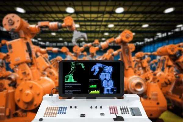
Routers and switches are essential devices in computer networks, allowing multiple devices to communicate and share resources efficiently. PCBs are used extensively in routers and switches to connect different components, manage power and heat, and ensure signal integrity.
Fiber optic communication equipment uses light signals to transmit information over long distances quickly and reliably. PCBs are crucial in fiber optic devices, supporting the optical components and connecting them to electronic circuitry.
Mobile base stations, also known as cell towers, are the backbone of mobile communication networks, enabling wireless communication between devices. PCBs play a critical role in base station design, providing the necessary connections between antennas, amplifiers, and other components.
TV satellite receivers are used to receive and decode television signals from satellites. PCBs are used in these devices to support the decoding process and provide interface connections to other devices, such as televisions and speakers.
Telephone systems use a combination of hardware and software components to enable voice communication over long distances. PCBs are used in telephones to connect the microphone, speaker, keypad, and other components, as well as to manage the power supply and signal processing.
As we can see, PCBs are essential in many different aspects of telecommunications and networking equipment, making them a crucial component in modern communication systems.
The design of a PCB is critical to the overall performance and reliability of the device it supports. In telecoms and networking equipment, where high-speed data transfer and signal integrity are paramount, PCB design plays an even more crucial role. Here are some important factors to consider when designing PCBs for telecoms and networking equipment:
The size and layout of a PCB can have a significant impact on its performance and functionality. Careful consideration of the component placement, trace routing, and layer stacking can help achieve better signal integrity, reduce noise, and optimize thermal management.
The choice of materials used in a PCB can also affect its performance and durability. High-quality materials, such as FR-4 fiberglass or ceramic, can provide better electrical properties and mechanical strength, leading to improved reliability and longevity.
Trace routing and layer stacking refer to the arrangement of copper traces and layers within a PCB. Proper trace routing can help maintain signal integrity, reduce crosstalk, and improve power distribution. Layer stacking can help with thermal management and reduce electromagnetic interference.
Power management and noise control are crucial considerations in PCB design. Proper power distribution and management can help prevent power loss or damage to components. Noise control measures, such as shielding and filtering, can reduce unwanted signals and improve signal quality.
Testing and validation are critical steps in ensuring the quality and reliability of a PCB. Various methods, such as functional testing, electrical testing, and environmental testing, can help identify any issues and ensure that the PCB meets the necessary standards and specifications.
There are several types of PCB used in telecommunications and networking equipment, each with its own advantages and applications. Here are some of the most common types:
Single-sided PCBs are the simplest type of PCB, consisting of a single layer of copper traces and components mounted on one side of the board. They are inexpensive, easy to manufacture, and suitable for low-density designs. However, single-sided PCBs are limited in their complexity and functionality.
Double-sided PCBs have two layers of copper traces and components mounted on both sides of the board, connected by vias or plated through holes. They provide more flexibility and space for circuit designs than single-sided PCBs while still being relatively easy to manufacture.
Multi-layer PCBs consist of multiple layers of copper traces and insulating material, sandwiched together and connected by vias or plated through holes. They provide even greater flexibility and space for complex circuit designs, as well as improved signal integrity and power distribution. However, they are more challenging and costly to manufacture than single-sided or double-sided PCBs.
Flexible PCBs, also known as flex circuits, are made of flexible materials, such as polyimide or polyester, that allow them to bend or conform to different shapes or surfaces. They are commonly used in applications where space is limited, such as mobile devices, cameras, or wearables.
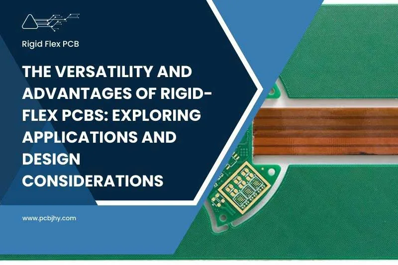
Rigid-flex PCBs combine the benefits of rigid and flexible PCBs, providing a flexible section and a rigid section on the same board. They offer greater flexibility and space for complex circuit designs than standard PCBs while maintaining durability and reliability.
High-frequency PCBs are designed to operate at frequencies above 1 GHz and are used in applications such as microwave communication, satellite communication, and radar systems. They require careful design and material selection to ensure optimal signal integrity and minimal loss.
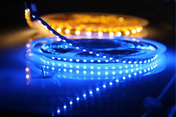
Metal core PCBs use a metal base instead of a traditional insulating substrate, offering better thermal management and heat dissipation capabilities. They are commonly used in applications with high-power components or where temperature control is critical, such as LED lighting or power electronics.
HDI (High-Density Interconnect) PCBs use advanced manufacturing techniques to create finer traces and spaces, allowing more components to be packed into a smaller area. They are commonly used in mobile devices, cameras, and other small form factor products.
Ceramic PCBs use a ceramic substrate instead of a traditional fiberglass substrate, providing excellent electrical and thermal properties. They are commonly used in high-frequency and high-temperature applications, such as power amplifiers, sensors, and automotive electronic modules.
By understanding the advantages and limitations of different PCB types, designers can select the most suitable type for their telecoms and networking equipment projects, depending on the specific requirements and constraints of the application.

PCB manufacturing can have a significant impact on the overall cost, production cycle time, and quality of telecoms and networking equipment. Here are some important factors to consider when it comes to PCB manufacturing:
The cost of PCB manufacturing can vary significantly depending on several factors, such as the size of the PCB, the complexity of the design, and the production volume. Working with a reliable PCB manufacturer can help reduce costs by optimizing the design for manufacturability and identifying cost-saving opportunities.
Production cycle time refers to the time taken to complete the entire PCB manufacturing process, from design to delivery. Shorter production cycle times can help reduce lead times and improve time-to-market for new products. Advanced manufacturing technologies, such as automated assembly and testing, can help shorten production cycle times.
PCB quality is critical in ensuring the performance and reliability of telecoms and networking equipment. Poor-quality PCBs can result in system downtime, loss of data, and even safety hazards. Working with a reputable PCB manufacturer that follows strict quality control measures can help ensure that the final product meets the necessary standards and specifications.
In conclusion, PCB manufacturing plays a vital role in the overall success of telecoms and networking equipment development. Partnering with a reliable PCB manufacturer that can provide high-quality, cost-effective, and timely solutions can help ensure that your project meets or exceeds its goals.
In conclusion, PCBs are an essential component of telecommunications and networking equipment, providing the necessary connectivity and support for other electronic components. Proper PCB design and manufacturing play a critical role in ensuring the performance, reliability, and cost-effectiveness of these devices.
By understanding the different types of PCB and their specific advantages and limitations, designers can select the most suitable type for their telecoms and networking equipment projects.
If you have any questions or inquiries about PCB design and manufacturing for your telecoms and networking equipment projects, please feel free to contact us at sales@pcbjhy.com or use our online inquiry form.
At JHYPCB, we provide high-quality, cost-effective, and timely solutions for all your PCB needs. Our advanced manufacturing capabilities and strict quality control measures ensure that your project meets or exceeds its goals.


When you partner with us, we do everything to ensure your PCB manufacturing and assembly are completed on time to your specifications with the highest quality.
Fill out the form below, and we will get back to you within the next 24
hours to complete the order, and then you’re all set to get started!