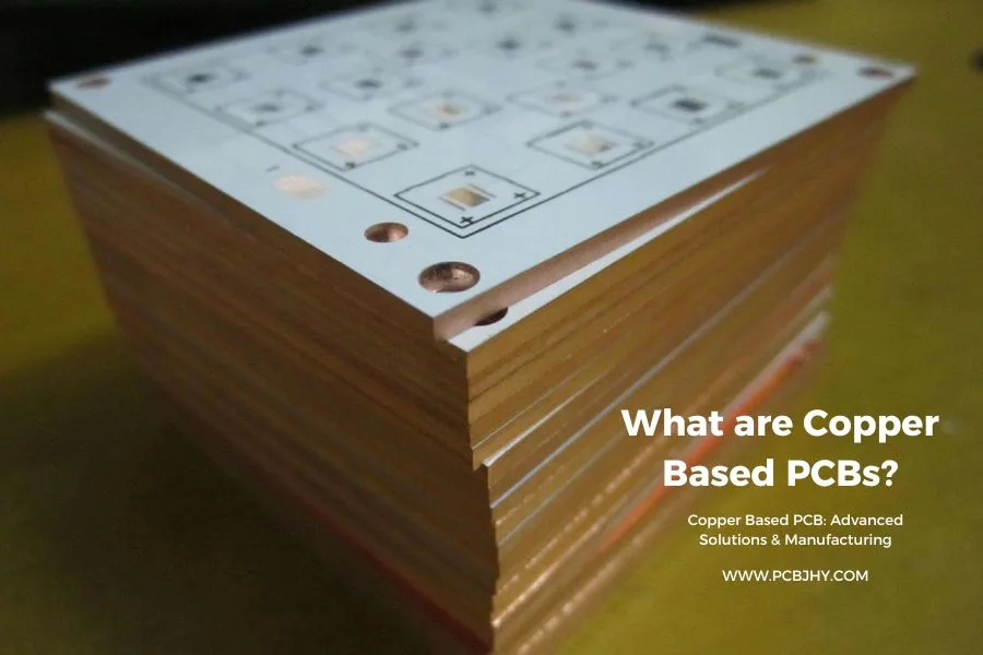
PCBs serve as the core foundation of electronics, providing the mechanical structure and electrical connections between components. They are found in practically every electronic device nowadays. Copper is the most commonly used conductor material in PCBs due to its highly suitable electrical and thermal properties.
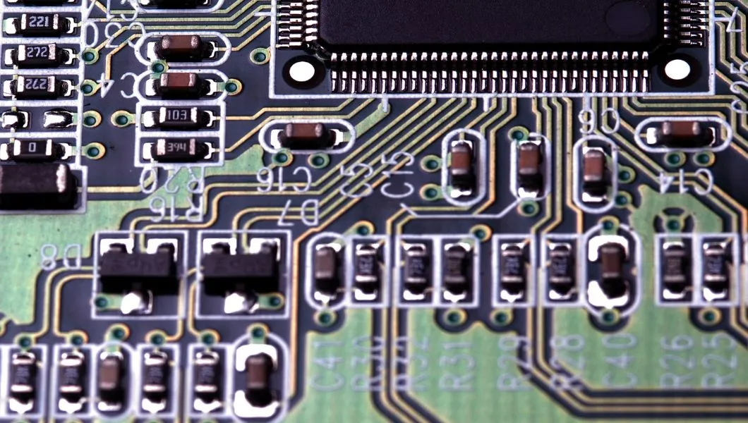
PCBs consist of insulating substrates laminated with thin conductive copper foil circuit patterns. The board is etched to form intricate copper tracings that interconnect components placed on the PCB surface. They provide signal transmission pathways as well as power and ground distributions.
Nearly all PCBs use copper for the conductive parts. This includes the tracks, pads, vias, and other metallic elements. Copper has become ubiquitous thanks to properties that make it exceptionally well-suited for printed circuits.
This article explores the key reasons why copper is the conductor material of choice in the fabrication of PCBs. We will examine the electrical, thermal, chemical, and economic factors that make copper ideal for printed circuit boards. An understanding of these benefits helps us appreciate why copper has become indispensable for modern electronics.
Basic PCB Materials
PCBs typically comprise four layers: substrate, copper foil, solder mask, and silkscreen. The substrate is the base layer, usually fiberglass, and supports the other layers. Copper foil is used for conductive traces and is the most critical material in PCBs. The solder mask protects the copper traces from oxidation and contamination, and the silkscreen is used for labeling and identifying the components on the board.
Why Choose Copper for PCBs?
Copper is the most commonly used material for the conductive traces in PCBs. Its use is primarily due to its high conductivity, low cost, and availability. Copper is an excellent conductor of electricity, which ensures that the signals transmitted through the board are not attenuated, leading to better signal integrity. Its high conductivity also means that less copper is required to achieve the same performance level, reducing the board’s overall cost.
Copper is also readily available, with many copper mines around the world. This abundance makes copper a cost-effective choice for PCB manufacturers.
Other Alternative Materials
While copper is the most commonly used material for PCBs, other materials can be used, depending on the application. Here are some alternative materials:
Aluminum: Aluminum is an alternative to copper for high-power applications, as it has better heat dissipation properties. However, it is not as conductive as copper, which limits its use in high-frequency applications.
Gold: Gold is an excellent conductor of electricity, and it is used in high-end PCBs, such as those used in aerospace and military applications. However, it is costly, which limits its use in consumer electronics.
Silver: Silver is another excellent conductor of electricity, but it is not as commonly used as copper or gold. It is mainly used in high-frequency applications like radio frequency (RF) circuits.
Conductive polymers: Conductive polymers are a relatively new material used in PCBs. They are flexible and can be molded into different shapes, making them ideal for flexible PCBs. However, their conductivity is not as high as copper, which limits their use in high-performance applications.
The role of copper in PCB
Copper has been the preferred material for PCBs for several decades. Copper is chosen for its excellent electrical conductivity, corrosion resistance, weldability, and ability to ensure high-performance circuits.
- Electrical Conductivity
Copper is the material of choice for printed circuit boards due to its high electrical conductivity. Electrical conductivity refers to a material’s ability to allow the flow of electric current. Copper has the second highest electrical conductivity among pure metals, after silver.
The high conductivity of copper allows printed circuit boards to effectively and efficiently transmit signals between different components and devices. When an electric current passes through a conductor like copper, some energy is inevitably lost in the form of heat. A material with high conductivity will have less electrical resistance and therefore less power loss.
Copper’s high conductivity ensures the required power flows through PCB tracks to power components, with minimal loss due to heat. This maximizes the operational efficiency of PCBs and prevents overheating issues. If the conductivity was poor, more power would be required to drive the same components and the increased heat generation could damage circuits.
Additionally, as copper PCB tracks can carry higher currents without voltage drop, PCBs can use thinner tracks, allowing more compact and higher density circuit designs. The excellent conductivity of copper has made it the conductor of choice for printed circuits right from the earliest days of PCB technology to the advanced PCBs found in modern electronics.
- High Thermal Conductivity
Copper’s excellent thermal conductivity also makes it well-suited for printed circuit boards. Thermal conductivity refers to a material’s ability to transfer heat. It is a very desirable property for PCBs.
The various electronic components on a printed circuit board generate heat during operation. If this buildup of heat is not quickly dissipated, it can cause components to malfunction or sustain permanent damage. Excessive heat can also cause issues like signal loss in interconnects and delamination of the laminated copper layers.
Here copper provides a major advantage. It has high thermal conductivity, second only to silver among pure metals. Copper can rapidly draw heat away from hot spots and spread it evenly across the PCB through its large surface area. This prevents localized overheating and failures.
With the help of heat sinks and fans, copper PCBs can maintain all components at safe operating temperatures. If the PCB substrate had poor thermal conductivity, the board would get excessively hot during high power operations. Devices could fail permanently or have decreased lifetime.
- Corrosion Resistance
Another major advantage of copper for printed circuit boards is its good corrosion resistance. When exposed to air, copper undergoes oxidation which forms a protective coating of copper oxide on the surface. This coating shields the underlying copper from further corrosion.
Oxidation is a concern with PCBs because even a small amount of corrosion can degrade the electrical performance of copper tracks. The oxidized coating limits this issue with copper. It maintains low electrical resistance and preserves the high conductivity needed for proper PCB operation.
Additionally, the oxide layer provides protection against common corrosive agents like moisture, salts and pollutants. This allows copper PCBs to better withstand day-to-day use in varied environments, from consumer electronics to industrial applications.
While silver is more conductive than copper, it lacks this corrosion resistance. PCB tracks made from silver would tarnish and degrade over time when exposed to air. Gold also readily corrodes in some environments.
Copper’s anti-corrosion property gives it an important advantage over other metals for long-term durability of PCBs. A slight amount of oxidation is unavoidable, but the oxide barrier ensures bulk conductivity remains intact. This enables reliable functioning over the entire lifespan of the PCB.
- Solderability
Copper also makes an excellent PCB substrate material due to its solderability – the ability to be joined with solder. This is a key requirement in PCB manufacturing.
Soldering is used to attach and electrically connect electronic components to the copper pads and traces on a PCB. This is done by melting solder to form an intermetallic bond between the solder and copper surfaces.
Copper readily reacts and bonds with typical solder materials like tin-lead or tin-silver-copper alloys. This allows components to make strong mechanical and electrical connections with copper tracings on PCBs.
Good solderability ensures the reliable assembly of surface mount and through-hole components onto printed circuit boards. It results in secure solder joints that do not easily crack or detach under mechanical or thermal stresses.
While metals like gold and silver have higher electrical conductivity than copper, they have poor solderability. Their smooth surfaces make it difficult to achieve adhesion with solder. Therefore copper’s advantage in soldering makes it a more practical metal for PCB substrates.
- Availability and Cost
Apart from its physical properties, the abundance and cost-effectiveness of copper also make it the ideal choice for printed circuit boards.
Copper is one of the most abundant metals available naturally. It is extensively mined and refined into high purity copper needed for electronics. The annual global copper production reached 20 million tonnes in recent years. This high availability ensures a stable supply even for large scale PCB manufacturing.
In addition, copper is relatively inexpensive compared to other highly conductive metals like silver, gold and platinum. Bulk industrial grade copper costs around $2.5 per pound. This low cost allows copper PCBs to be fabricated economically in very high quantities.
Using silver circuits could enhance conductivity but would be prohibitively expensive. Gold plating is used sparingly on connection points and traces requiring maximum reliability. Widespread use of gold or silver throughout PCBs is not feasible economically.
The affordability and abundance of copper has made printed circuit boards viable for a wide range of electronics, from mass consumer devices to specialty industrial equipment. This has fuelled the electronics revolution and growth of computing technology over the past decades.
copper thickness in PCB
PCB copper thickness is an essential factor to consider when designing a printed circuit board. The copper thickness determines the current carrying capacity, mechanical strength, and cost of the PCB.
- Importance of Copper Thickness
The thickness of the copper layer on a PCB is critical to the board’s performance. The copper layer’s thickness determines how much current can flow through the board without causing excessive heating or voltage drop. The thickness also affects the mechanical strength of the board, as a thicker copper layer provides better adhesion and resistance to wear and tear. The thickness of the copper layer can also affect the cost of the PCB, as thicker layers require more copper and manufacturing time.
- Measuring Copper Thickness
The thickness of the copper layer on a PCB can be measured using several techniques, including destructive and non-destructive methods. Destructive methods involve removing a small portion of the copper layer and measuring its thickness using a microscope or a micrometer. Non-destructive methods include eddy current measurement, X-ray fluorescence, and beta backscatter. These methods provide a more accurate measurement of the copper thickness without damaging the PCB.
- Standard Copper Thicknesses
PCB manufacturers offer several standard copper thicknesses, ranging from 0.5 oz to 10 oz. The thickness is expressed in ounces per square foot, with 1 oz equivalent to 1.4 mils or 35 µm. The standard copper thicknesses are shown in the table below.
| Copper Weight | Copper Thickness |
|---|---|
| 0.5 oz | 0.7 mils / 17 µm |
| 1 oz | 1.4 mils / 35 µm |
| 2 oz | 2.8 mils / 70 µm |
| 3 oz | 4.2 mils / 105 µm |
| 4 oz | 5.6 mils / 140 µm |
| 5 oz | 7.0 mils / 175 µm |
| 6 oz | 8.4 mils / 210 µm |
| 10 oz | 14.0 mils / 350 µm |
- Impact on Performance
The copper thickness on a PCB has a direct impact on the board’s performance. A thicker copper layer provides a lower resistance path for the current, leading to a higher current carrying capacity and reduced voltage drop. It also provides better mechanical strength and improved resistance to wear and tear. However, a thicker copper layer can also increase the manufacturing cost of the board and make it more challenging to solder components to the board. Additionally, thicker copper layers may require more current to etch, leading to longer etching times and higher manufacturing costs.
Copper in Heavy Copper PCB
Heavy copper PCBs are printed circuit boards that have copper traces and planes that are thicker than those found on regular PCBs. These boards are often used in high power applications, where they can handle higher currents and dissipate more heat than standard PCBs. The relationship between heavy copper PCBs and copper is evident in the board’s design and manufacturing process.
Heavy copper PCBs are designed to have thick copper traces and planes. The thickness of the copper layer can range from 2 oz to 20 oz or more, depending on the application’s requirements. The thickness of the copper layer directly affects the board’s performance, as thicker copper layers provide lower resistance paths for the current, reducing voltage drop and improving power dissipation. The copper layer’s thickness can also affect the board’s mechanical strength, making it more resistant to wear and tear.
To manufacture heavy copper PCBs, specialized equipment and techniques are required. The process involves starting with a copper-clad laminate, which is then coated with a layer of photoresist. The photoresist is then exposed to UV light through a photomask, which defines the circuit pattern. The exposed photoresist is then developed, leaving behind the circuit pattern on the copper layer. The unmasked copper is then etched away using an etchant solution, leaving behind the copper traces and planes.
The etching process for heavy copper PCBs can be more challenging than for standard PCBs due to the thicker copper layers. The etchant solution must be more aggressive, and the etching process may take longer to complete. The process can also be more expensive, as more copper is required to produce the board, and the manufacturing process may take longer.
Here is a table showing perfomance for copper in heavy copper PCBs:
| Property | Value |
|---|---|
| Copper weight (oz) | 2-20 or more |
| Maximum current carrying capacity (A) | Up to 300 |
| Thermal conductivity (W/mK) | 400 |
| Coefficient of thermal expansion (ppm/°C) | 16-18 |
| Surface finish | Immersion gold, ENIG, OSP, HASL |
| Solderability | Good |
| Corrosion resistance | Excellent |

