PCB Prototypes: The Essential First Step for Successful Product Development
When it comes to developing new electronic products, having a fully functional printed circuit board prototype is absolutely critical before moving to full production. A PCB prototype allows you to thoroughly test and validate your design, identify any issues early on, and make necessary modifications before committing to a costly high-volume manufacturing run.
In the fast-paced world of electronics, being first to market with a new product can be the difference between success and failure. PCB prototyping services enable you to quickly iterate on designs, explore different layout options, and experiment with various components and materials. This agile process ensures your final PCB is optimized for performance, reliability, and cost-effectiveness right from the start.
Whether you’re working on a simple single-sided PCB or a complex high-density interconnect board, PCB prototyping is an indispensable stage. From rigid PCB boards to flexible circuits and aluminum substrate PCBs, there is a prototyping solution tailored for every PCB type and product need. Multilayer PCB prototypes, rigid-flex PCB prototypes, and HDI PCB prototypes are just a few of the common PCB prototypes used across industries.
So what exactly is involved in PCB prototyping? In this comprehensive guide, we’ll dive deep into the world of PCB prototypes – exploring the different types, the prototyping process, costs, and how to select the right PCB prototype manufacturer for your needs. Whether you’re based in the United States, China, Europe, or anywhere else globally, this guide will equip you with everything you need to know about PCB prototyping.
What is a PCB Prototype?
A PCB prototype is an initial physical model or sample of a printed circuit board design. It serves as a crucial bridge between the design phase and full production, allowing engineers and developers to test, validate, and refine their PCB before committing to mass manufacturing.
Definition of a PCB Prototype
A printed circuit board prototype is an early maker-built version of the final PCB product. It brings the theoretical design into a tangible form factor for evaluation. PCB prototypes enable hands-on testing of form, fit, and function under real operating conditions.
Different Types of PCB Prototypes
There are various types of PCB prototypes to meet the diverse needs of electronic products across industries:
- Single/Double-Sided PCB Prototypes: These are the most basic prototypes with components on one or both sides of the board, suitable for simple, low-density circuit designs.
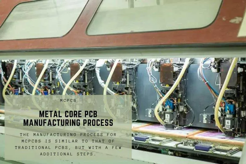
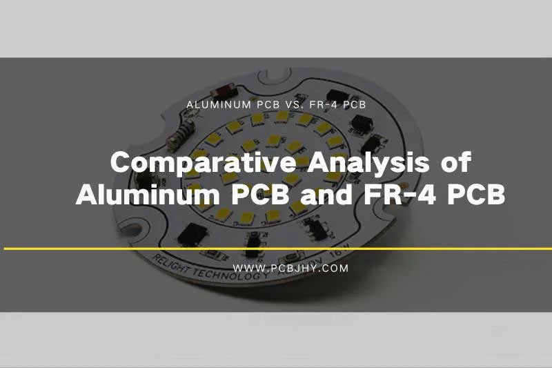
- Aluminum/Metal Core PCB Prototypes: These utilize aluminum or other metal substrates instead of the traditional FR-4 material. Metal-core PCBs offer superior thermal dissipation for high-power applications.
- Multilayer PCB Prototypes: With conductor layers stacked and interconnected, multilayer PCBs accommodate higher component densities while minimizing trace lengths for improved signal integrity.
- Flexible PCB Prototypes: Made by adhering flexible laminates, these allow for unique form factors in compact or dynamically flexing product designs.
- Rigid-Flex PCB Prototypes: Combining rigid and flexible board sections, these enable the integration of PCBs into non-planar product enclosures.
- HDI PCB Prototypes: High-Density Interconnect PCBs utilize advanced fabrication to achieve extremely high wiring densities, ideal for today’s miniaturized electronics.
Common PCB Prototype Applications
Across sectors like consumer electronics, industrial equipment, aerospace, automotive, medical devices and more, PCB prototypes are indispensable for:
- Design verification and validation testing
- Form factor evaluation and fit checks
- Environmental and reliability stress testing
- Regulatory compliance and certification testing
- Small production runs before full scale-up
Whether it’s a simple single-layer PCB board or a complex high-speed HDI design, getting a prototype built is crucial for ensuring a successful PCB product launch. The ability to physically test and optimize a PCB before production can prevent very costly mistakes.
The PCB Prototyping Process
Now that we’ve covered the different types of PCB prototypes, let’s dive into the prototyping process itself. Transforming your PCB design into a functional physical prototype involves several key steps:
PCB Design
The prototyping process begins with your PCB design files, typically Gerber files outputted from PCB design software like Altium, Cadence, or KiCad. These files contain all the copper layer patterns, drill holes, solder masks, and silkscreen details to fabricate the bare PCB.
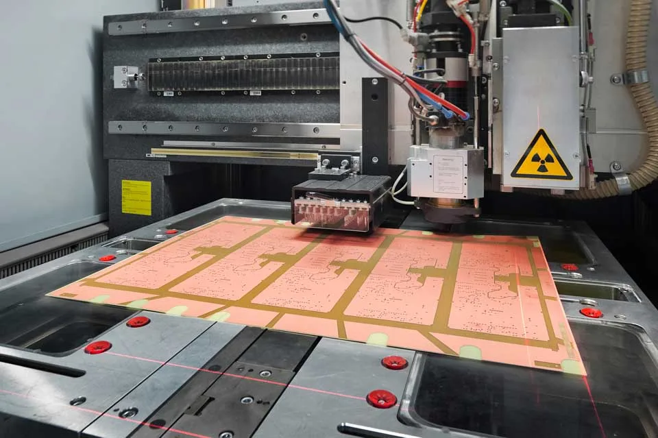
PCB Fabrication
Once the design files are ready, they are sent to a PCB prototype manufacturer. Using your files as the blueprint, the bare PCB is fabricated through processes like:
- Imaging: Laser-printing the circuit patterns onto photosensitive films
- Etching: Removing unwanted copper to form the traces and features
- Lamination: For multilayers, bonding individual circuit layers together
- Drilling: Creating holes for component leads and interconnect vias
- Plating: Applying a conductive surface finish like ENIG, HASL or immersion silver
This fabrication transforms the design into a physical bare PCB panel or array ready for assembly.
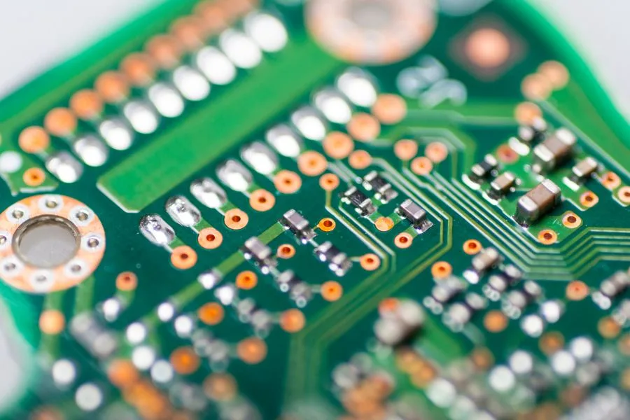
The bare PCB prototype then moves to the assembly phase where components are installed:
- Solder paste printing: Depositing solder onto the PCB pads
- Component placement: Using automated pick-and-place machines
- Reflow soldering: Melting the solder to make permanent connections
- Secondary processes: Like surface mount device inspection, conformal coating, etc.
Electrical testing is performed on assembled prototypes to ensure functionality matches the design intent. If issues are found, designers can identify the root cause and quickly iterate on the design before the next prototype spin.
Quick-turn PCB prototyping services can produce assembled PCB prototypes in as little as 24-72 hours. This accelerated prototyping process enables much faster product development cycles compared to traditional methods.
In addition to allowing design verification, PCB prototypes are essential for:
- Testing manufacturing processes and assembly workflows
- Evaluating thermal, RF, EMC, and environmental performance
- Qualifying new components, materials, or design techniques
- Regulatory, compliance, and certification testing
By going through comprehensive prototyping, you can fully validate your PCB design and pre-production processes. This mitigates risks and ensures a smooth, cost-effective transition to volume manufacturing.
PCB Prototype Pricing and Costs
One of the key considerations for any product development project is budget. When it comes to PCB prototypes, pricing can vary significantly based on a number of factors. Understanding what impacts PCB prototype costs is important for proper planning and avoiding sticker shock.
Factors Affecting PCB Prototype Pricing
- Board Size and Layer Count – Larger boards with more copper layers are more expensive
- Board Type – HDI, rigid-flex, aluminum PCBs cost more than standard FR4 PCB boards
- Material Type – Higher quality laminates and specialized materials increase costs
- Quantity – Pricing is per panel or array, so higher quantities mean higher costs
- Turnaround Time – Quicker TAT services like 24-hour PCB prototyping cost a premium
- Design Complexity – Dense BGAs, micro vias, blind/buried vias add complexity
- Assembly Requirements – More components, mixed technology, special processes
- Geographical Location – Pricing can differ between countries like China, USA, Germany etc.
Example PCB Prototype Pricing To give you a sense of typical pricing, here are some example costs for common PCB prototypes:
- 4″ x 6″ double-sided PCB, HASL, 5-7 day TAT: $100-$300 per panel
- 6″ x 8″ 6-layer PCB, ENIG, 72-hour TAT: $300-$600 per panel
- 10″ x 12″ HDI prototype, 8+ layers, quick turn: $1,000-$2,500 per panel
- Rigid-flex PCB prototype with stiffeners: $800-$1,500 per array
These are just rough estimates as actual pricing depends on the specific requirements. For low volume production runs beyond prototyping, PCB costs decrease substantially due to economies of scale.
Many prototype PCB manufacturers provide free quoting tools on their websites for convenience. Getting a formal quote with pricing details is recommended before moving forward.
Working with an experienced PCB prototype partner can also ensure you receive good value through techniques like:
- Panel maximization to increase design utilization
- Pre-production Supply Chain assessment to control future costs
- Design for Manufacturing (DFM) advice to reduce complexity
While PCB prototypes come at a premium, they represent a small fraction of overall product development costs. The investment in comprehensive PCB prototyping ensures your final design is optimized for performance, quality and cost-efficiency.
Selecting the Right PCB Prototype Manufacturer
With the importance of PCB prototyping established, the next critical step is finding a capable manufacturing partner to produce your prototypes. There are many PCB prototype manufacturers to choose from globally, so doing your research is crucial.
Major PCB Prototype Manufacturers Some of the leading companies providing PCB prototyping services include:
- PCBWAY (China)
- JHYPCB (China)
- Sierra Circuits (USA/Mexico)
- Wizlogix Pte Ltd (Singapore)
- Genus Electrotech (India)
- AIRPRO (Taiwan)
- European Circuits (UK/Europe)
- AT&S (Austria)
These are just a few of the many PCB prototype houses operating worldwide. Capabilities can vary significantly between different manufacturers.
Key Considerations When Evaluating Manufacturers
- Prototyping Capabilities – Ensure they can fabricate your required PCB type, layers, materials etc.
- Advanced Technologies – HDI, rigid-flex, aluminum, RF/microwave capabilities if needed
- Quick-Turn Options – Availability of 24-hour to 5-day rapid PCB prototype manufacturing
- Engineering Support – DFM feedback and pre-production expertise
- Quality Certifications – ISO 9001, AS9100, MIL-PRF-31032, TS16949 etc.
- Global Locations – Manufacturing sites in your major markets like China, USA, Canada, Europe
- Pricing Structure – Get full quotes detailing costs for your design and requirements
Many companies offer free app-based PCB quote calculators to get pricing estimates easily.
Customer Reviews and Recommendations In addition to technical capabilities, also consider customer satisfaction ratings and reviews for qualities like:
- Responsiveness and communication
- Order accuracy and quality consistency
- Adherence to committed lead times
- Problem resolution and customer support
Referrals from other electronics companies can provide valuable insight as well.
For early-stage prototyping, working with a local manufacturer may be preferred for ease of communication. But high-volume production may require globally-based manufacturers offering more economies of scale.
Ultimately, selecting the right PCB prototype partner is about finding the best combination of technical capabilities, pricing, operational expertise, and customer focus aligned with your project needs. Proper vetting upfront prevents headaches during your development cycle.
As the world’s manufacturing hub, China has emerged as a dominant force in the PCB prototyping industry as well. Several factors have fueled China’s lead in this domain:
- Massive Scale – China’s enormous production capacities, from PCB board fabrication to component sourcing to assembly, enable fast, cost-effective PCB prototyping.
- Technological Leadership – Many Chinese PCB manufacturers have made huge investments in advanced technologies like HDI, rigid-flex, and lower micron processes.
- Established Supplier Base – China’s vast base of EMS companies provides robust domestic supply chains and logistics for prototyping.
- Cost Advantages – With access to lower-cost materials and labor, Chinese suppliers can offer very competitive PCB prototype pricing.
- Notable Players – Top Chinese firms like PCBWAY, JHYPCB, Rayming, and ALLPCB are prototyping leaders.
The United States also has a well-established PCB prototyping industry serving the needs of companies locally as well as globally. Several advantages make American manufacturers an attractive choice:
- Advanced Capabilities – Leading US PCB shops like Sierra Circuits, Sunstone Circuits, and Coast2Coast Circuits offer cutting-edge prototyping for HDI, rigid-flex, RF/microwave, aluminum, and IC substrate PCB types.
- Quick Turnarounds – With domestically-based fabrication and assembly, rapid PCB prototyping services with 24-72 hour lead times are readily available.
- Engineering Support – Top US facilities provide skilled DFM expertise to optimize designs for prototype and production.
- High Quality/Reliability – Stringent quality and reliability standards governed by certifications like MIL-PRF-31032 and AS9100.
While pricing may be higher compared to lower-cost regions, the combination of advanced capabilities, quick cycles, engineering collaboration and quality focus makes American PCB prototyping very attractive for many OEMs. Proximity to the massive US electronics market is another advantage.
Many prominent companies like Apple, Cisco, Lockheed Martin and more rely on American PCB prototype manufacturers, especially for high-reliability aerospace, defense and medical applications where quality is paramount.
So for products requiring ultimate quality, cutting-edge technologies, and tight engineering integration, USA-based PCB prototype manufacturing could be the ideal solution.
PCB Prototyping in Major European Countries (UK, France, Germany)
Europe is another key region for PCB prototype manufacturing, with hubs in countries like the United Kingdom, France, and Germany serving the needs of OEMs across the continent.
United Kingdom (PCB Prototype UK)
While not as large as China or the USA, the UK has a solid PCB prototyping industry centered around manufacturers like:
UK suppliers excel at rapid quick-turn PCB prototyping services, with many offering 24-72 hour lead times. Their close proximity to customers enables tight communication loops.
France (PCB Prototype France)
Major PCB fabricators in France include:
In addition to PCB prototypes, many are geared towards low-to-medium volume production runs. Leading-edge HDI capabilities are a strength.
Germany (PCB Prototype Germany)
As a global manufacturing powerhouse, Germany is also home to several premiere PCB prototype companies such as:
German manufacturers are known for their engineering precision and quality focus, making them a favored choice for high-reliability applications.
Across the UK, France, and Germany, domestic manufacturers provide localized manufacturing with the advantages of reduced logistics costs and shorter shipping timelines for European OEMs. However, offshoring PCB prototypes to lower-cost regions is still common for cost-sensitive projects.
Other Regional PCB Prototyping Hubs
While China, the USA, and Europe are major PCB prototyping hubs, many other countries and regions have emerged with strong capabilities as well. Here’s a look at some key players:
Canada (PCB Prototype Canada)
Top Canadian PCB prototype manufacturers include:
With quick-turn options and domestic production, they serve OEMs across Canada as well as the United States market. Advanced HDI and flex capabilities are strengths.
Taiwan (PCB Prototype Taiwan)
Taiwan is an island of PCB manufacturing excellence with firms like:
Benefiting from established semiconductor ecosystems, these manufacturers offer cutting-edge HDI, SLP, and IC substrate prototyping solutions.
Other Asia (PCB Prototype Singapore, Malaysia, India etc.)
Countries like Singapore, Malaysia, India, South Korea and Japan also host regional PCB prototype manufacturers such as:
- Integrated Microwave Corp (Malaysia)
- Numerical Circuits (India)
- GEML Circuits (Singapore)
These provide localized low-cost prototyping for OEMs operating in these markets.
While limitations exist in some geographies on advanced PCB types, manufacturers in many regions can produce high-quality basic prototypes very cost-effectively.
This global PCB prototyping landscape gives OEMs the flexibility to choose partners that best fit their technical requirements, budgets, and supply chain needs for each product program.
FAQ about PCB Prototypes
Most rigid PCBs utilize fiberglass-reinforced epoxy laminate substrates like FR-4. Flexible PCBs use polyimide or polyester films. Advanced PCBs may use specialized materials like Rogers, Polytetrafluoroethylene (PTFE) or aluminum/metal cores.
Soldering is the process of forming permanent electro-mechanical interconnections between PCB pads and component leads/terminations. The two main soldering methods are wave soldering for through-hole components and reflow soldering for surface mount devices.
Printed circuit boards provide the foundational interconnection routing and mechanical mounting for all electronic components and circuits in virtually any electronic product from consumer devices to industrial equipment.
HDI (High Density Interconnect) PCBs utilize advanced fabrication techniques like microvias, buried vias and higher connection densities to route extremely high wiring densities for today's highly integrated and miniaturized electronics.
Key advantages of PCB Prototype include:
- Verifying the design and catching issues early
- Testing circuit and product performance
- Evaluating manufacturing process feasibility
- Optimizing the design for quality and cost-effectiveness
- Supporting low volume production runs
Standard lead times are typically 5-10 business days, but quick-turn prototyping services can produce prototypes in as little as 24-72 hours.
Prototypes are low volume samples used for evaluation and testing. Full production is the high-volume manufacturing run of the finalized design.
Common surface finishes include:
- HASL (Hot Air Solder Leveling)
- ENIG (Electroless Nickel Immersion Gold)
- Immersion Silver
- OSP (Organic Surface Protectant)
- ENEPIG
Some methods are using standard materials/specs, optimizing design complexity, maximizing design utilization, and negotiating with manufacturers.
For most new designs or major revisions, prototyping is essential. But for minor ECO changes, analysis can determine if a new prototype spin is required.
Accelerating Product Development with PCB Prototypes
As we’ve covered throughout this guide, PCB prototyping is an absolutely essential step for successful product development and launch. From initial design verification to manufacturing process validation, having functional board prototypes is critical before committing to volume production.
The ability to quickly iterate through multiple prototype spins allows you to fully test, troubleshoot, and optimize your PCB design upfront. This mitigates risks and costly reworks later on. Leading OEMs across consumer electronics, industrial, automotive, aerospace, medical and other sectors rely on comprehensive PCB prototyping for their most innovative products.
Whether you require basic prototypes or need to leverage advanced technologies like HDI, rigid-flex, aluminum/metal core or high-frequency RF designs, there are proven PCB prototype manufacturers globally that can meet your needs. Choosing the right partner based on technical capabilities, quality focus, pricing and geographic advantages is vital.
From industry hubs in China, USA and Europe to emerging lower-cost regions, this guide has equipped you with an understanding of the vast PCB prototyping landscape available. You now have the knowledge to properly evaluate manufacturers and select sources fitting your unique project requirements.
At JHYPCB, we take immense pride in our ability to produce high-quality PCB prototypes across the entire spectrum of technologies. With AAAA certifications and adherence to stringent DFM principles, we provide not just prototypes but a true partnership for success through the entire product development lifecycle.
Ready to accelerate your product development with cutting-edge PCB prototypes? Contact us today for a free consultation, and let our team of experts guide you through the prototyping process. Leverage PCB prototypes as the critical enabler to bring your ambitious product visions to market quickly and cost-effectively.
Related Posts
- How to Get a Fast PCB Prototype: Tips and Strategies
- Affordable PCB Prototyping: Options Worldwide
- What is a Custom PCB?
- Key Factors Influencing Bare PCB Manufacturing Costs
- How to Select the Right Provider for Cheap PCB Prototypes – Key Evaluation Criteria
- The Rainbow of PCBs: A Guide to Solder Mask Colors and Their Uses