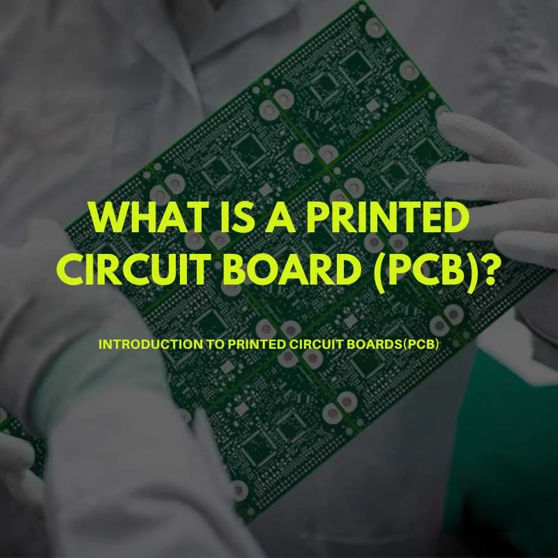
Introduction
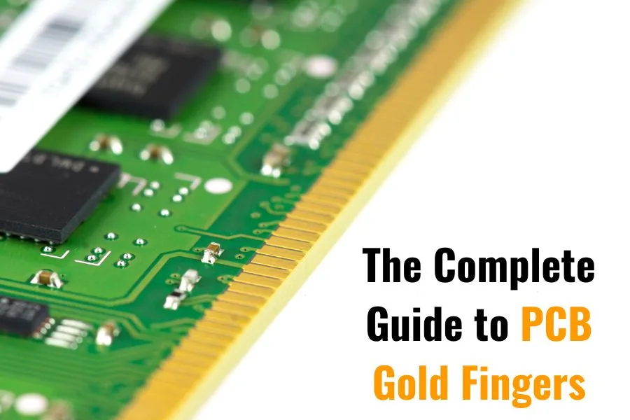
Gold fingers are those small gold-plated contacts along the edge of printed circuit boards that allow detachable connections for add-on cards and memory modules in computers and other devices. With the right design and manufacturing, gold fingers can provide reliable connectivity and stand up to thousands of insertion cycles. This complete guide to PCB gold fingers will cover everything you need to know about their purpose, optimal design considerations, manufacturing processes, inspection methods, and maintenance best practices.
With increasingly complex electronics and miniaturization, high-quality and durable gold fingers are essential for the performance and longevity of PCBs in products we use every day. Following the recommendations in this guide, you’ll understand what gold fingers are, why PCB designers specify them, and how to manufacture gold fingers that maximize conductivity, minimize wear, and avoid common defects.
We’ll discuss crucial design choices like finger positioning, size, pitch, and plating thickness that impact the reliability of gold fingers over thousands of insertion cycles. You’ll learn about advanced manufacturing processes like ENIG and ENEPIG plating that create uniform, defect-free gold fingers to meet functional requirements. We’ll also cover visual inspection techniques, continuity and plating thickness testing, troubleshooting steps, and maintenance procedures to keep gold fingers working properly after assembly and during use.
Whether you’re a PCB designer considering gold fingers for an upcoming project or a manufacturer tasked with producing defect-free gold fingers, this guide brings together industry best practices to optimize gold finger longevity, conductivity, and performance. Follow along as we dive into the essentials of PCB gold fingers.
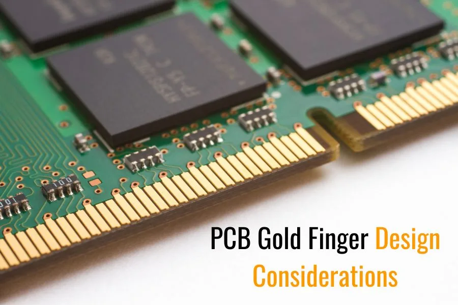
What are PCB Gold Fingers and Why Are They Used?
Gold fingers are the small, gold-plated copper traces along the edge of printed circuit boards that allow the PCB to make electrical contact with a connector or socket on another board or component. The gold plating ensures high conductivity while also resisting corrosion and abrasion over thousands of insertion cycles.
Gold fingers are typically designed as protruding tabs, strips, or leads on the PCB edge that align precisely with the contacts in the receiving connector or socket. The stiffness of the gold-plated fingers allows them to maintain constant pressure and connectivity when inserted, while the gold-plating provides excellent electrical conductivity even at low contact forces.
Some of the major advantages of using gold fingers on PCBs include:
- High durability – Gold plating resists corrosion and abrasion, allowing gold fingers to retain conductivity over long-term use.
- Low contact resistance – Gold provides very low electrical resistance, maximizing signal integrity at finger connections.
- High cycle life – Gold fingers can withstand thousands of insertion cycles without degrading.
- Gas tight connections – Gold fingers form gas tight connections with contact sockets, preventing oxidation.
- Easy wiping – Gold coating enables fingers to be wiped before insertion to remove contaminants.
- Solderless assembly – Gold fingers allow PCBs to be interconnected without soldering.
Common applications where gold fingers are essential include:
- Memory module DIMMs – Gold fingers allow easy insertion into DIMM sockets on motherboards.
- Add-on boards – PCI cards, graphics cards, network cards use gold fingers for motherboard slots.
- Board-to-board connectors – Gold fingers enable demountable connections between PCBs.
- Testing fixtures – Gold fingers used for repeatable device testing and programming.
For demanding electrical connections, gold fingers are often the optimal choice due to their durability, conductivity, and longevity over thousands of mating cycles.

PCB Gold Finger Design Considerations
Careful design is crucial for gold fingers to function properly and endure repeated insertions and removals over long-term use. Some key gold finger design choices include:
Positioning and Layout – Fingers should be positioned along the PCB edge in the exact footprint and spacing required to align with the receiving connector. Common layouts include single row or dual row fingers.
Pitch Size – The center-to-center spacing between adjacent fingers is known as pitch. Common pitch sizes range from 1.0mm to 0.4mm. Smaller pitches allow more contacts in constrained areas. Standards exist for common interfaces (e.g. JEDEC for DIMMs).
Copper Thickness – The underlying finger copper should be thick enough to resist warping and wear, typically at least 0.5 oz (18 microns) copper thickness.
Plating Thickness – The gold plating should be between 1-4 microns. Thicker plating increases cost but minimizes wear over more insertions.
Masking – Solder mask should be applied to avoid shorting between fingers during assembly, but removed from the contact area.
Additionally, factors like finger length, width, and gold plating purity (hard gold vs soft gold) impact performance. Too thin of gold risks corrosion and shorts while too soft allows excessive material transfer and buildup on mating connectors.
Ideally, gold finger design should maximize conductivity and durability while minimizing cost. Validation testing is recommended to ensure the design withstands vibration, thermal cycling, and repeated insertions without degradation or electrical issues.
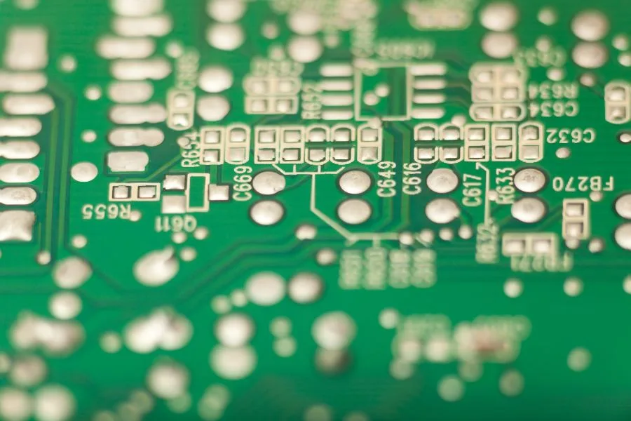
Manufacturing High-Quality Gold Fingers
The manufacturing process is crucial for producing defect-free gold fingers with proper plating thickness and consistency. Common plating methods include:
- ENIG (Electroless Nickel Immersion Gold) – Provides excellent wear resistance. Electroless nickel is deposited first, followed by an immersion gold overplate.
- ENEPIG (Electroless Nickel Electroless Palladium Immersion Gold) – Palladium layer provides excellent diffusion barrier prior to gold plating.
- Immersion Gold – Simple process with gold deposited directly over copper. Risk of migration issues over time.
- Hard Gold Plating – Nickel underplating with a gold alloy overplate creates a harder, more wear-resistant finger surface.
Key factors in gold finger plating include:
- Uniform Thickness – The plating thickness should be consistent across all fingers to prevent uneven wear or early failure.
- Minimizing Pits and Nodules – The plating should fully cover the copper without defects that allow corrosive migration under the gold.
- Adhesion – Proper prep and plating ensures the gold adheres properly to the finger base metal.
- Foldover Control – Proper masking prevents gold folding over the edges to avoid shorts between fingers.
Inspection methods such as visual checking, X-ray imaging, and plating thickness testing validate manufacturing quality. Following established standards like IPC or military specifications reduces defects.
Careful process controls, surface preparation, bath chemistry monitoring, and inspections help ensure reliable, high-performance gold fingers suitable for the application.

Testing, Inspection and Maintaining Gold Fingers
Once gold fingers are manufactured, rigorous testing and inspection helps verify their functionality and long-term reliability:
Continuity Testing – Checks for electrical shorts or opens before assembly by probing individual fingers or scanning connectors.
Plating Thickness – Measurement using X-ray fluorescence or eddy current sensors ensures proper plating depth.
Visual Inspection – Microscopic checking that the gold plating meets specifications and is free of defects or contamination.
Insertion Testing – Validates successful connectivity by mating with sockets through repeated insertions and removals.
Gold fingers should also be properly maintained after assembly to keep connections clean and prevent degradation:
- Cleaning – Wiping fingers with isopropyl alcohol helps remove oils, flux, and other contaminants.
- Proper Handling – Avoid touching gold fingers to minimize transfer of dirt, salts, and moisture.
- Re-Plating – In some cases re-plating may be warranted if the gold layer becomes excessively worn or corroded.
- Periodic Inspection – Visual checks and continuity testing helps spot issues with gold fingers early.
Proper insertion techniques are also important to avoid damaging gold fingers – keeping them straight when inserting and removing, avoiding bending or twisting. Early detection of any plating issues, dirt buildup, or loss of tension can maximize gold finger lifespan.

Gold Finger Design and Manufacturing Mistakes to Avoid
While high-quality gold fingers rely on rigorous design and manufacturing controls, there are some common errors and issues to be aware of:
- Insufficient Finger Length – Shorter fingers increase risk of misalignment and lose contact pressure during insertion.
- Inadequate Pitch Size – Crowding fingers too close together increases crosstalk and insertion force.
- Plating Foldover – Masking issues cause gold to wrap over finger edges, potentially causing shorts.
- Base Metal Exposure – Missing gold plating leads to corrosion and interrupted conductivity.
- Plating Voids – Missing plating in spots due to surface contamination or process issues.
- Nodules and Pitting – Small defects in the gold layer accelerate wear and corrosion.
- Non-Uniform Plating – Inconsistent plating thickness can lead to early failure of thinner fingers.
- Microcracks – Small fissures in the gold provide paths for corrosion migration under the plate.
- Gold Transfer – Excessively soft gold leads to material wiping off onto mating connectors.
- Handling Damage – Fingerprint residues, scratches, or bends during handling reduce reliability.
By following design guidelines and validating processes through testing, many gold finger issues can be prevented. Periodic inspection after assembly also helps detect any emerging issues early.
Conclusion
In summary, properly designed and manufactured gold fingers are crucial for maximizing the conductivity, durability, and performance of printed circuit board interconnections.
Following the recommendations in this guide for optimal finger layout, plating processes, inspection methods, and maintenance procedures will help prevent many of the potential defects and failure modes of gold fingers.
Some key takeaways include:
- Position gold fingers precisely to align with mating connectors and sockets.
- Choose suitable gold plating thickness, hardness, and uniformity.
- Validate manufacturing quality through visual, X-ray, and testing inspection.
- Protect gold fingers from contamination before and after assembly.
- Use proper insertion and removal techniques to avoid finger damage.
- Perform periodic cleaning, testing, and inspection to identify any emerging issues.
At JHYPCB, we have extensive experience manufacturing high-quality PCBs with reliable, defect-free gold fingers for a wide range of applications. Our rigorous quality control and inspection processes ensure that the gold fingers we produce meet or exceed the most demanding mechanical and electrical requirements.
Contact us today to discuss your next PCB gold finger project. JHYPCB can help assess design requirements, recommend optimal gold finger solutions, and deliver proven manufacturing expertise for your application needs.
Related Reading

What is PCB Gold Fingers: The Complete Guide
What are the Single Layer PCB Types?