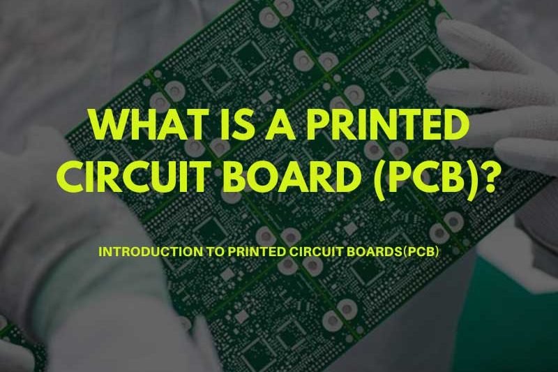
A Printed Circuit Board is an essential component in the manufacturing of electronic devices. It is a thin board made of insulating material, such as fiberglass or plastic, with conductive pathways etched onto its surface. The conductive pathways, or tracks, connect the electronic components and allow the flow of electricity. PCBs provide a reliable and efficient means of connecting electronic components and provide a platform for the creation of complex electronic circuits.
Table of Contents
What is a PCB?
A printed circuit board, commonly referred to as a PCB, is a board made of insulating material (typically fiberglass or plastic) with conductive pathways etched onto its surface. These pathways connect various components, such as resistors, capacitors, and integrated circuits, that make up an electronic device. The use of a PCB allows for compact and efficient assembly of electronic components, as well as a reduction in the amount of wire and cabling needed compared to older wiring methods. The design and manufacture of PCBs involves a complex process that includes laying out the electrical pathways, printing the pathways onto the board, drilling holes for components, and soldering components into place.
History of Printed Circuit Boards
The history of Printed Circuit Boards dates back to the early 1900s when electrical engineers first started exploring the idea of using metal strips to connect electronic components. Over the years, technology has evolved and improved, and PCBs have become an essential component of modern electronics.
One of the earliest examples of a PCB was a circular board developed by Paul Eisler in 1936 for use in a radio set. This board used a metal layer and an insulating layer to create electrical pathways, and it was a significant improvement over the point-to-point wiring methods that were previously used.
In the 1950s, the use of PCBs became more widespread as the electronics industry began to grow and more complex circuits were developed. During this time, the manufacturing process for PCBs was also refined, and the use of automated assembly methods became more common.
In the 1960s and 1970s, the development of microelectronics and the growing demand for smaller, more compact electronics led to further improvements in PCB technology. The use of multilayer printed circuit boards and the introduction of surface mount technology (SMT) allowed for the creation of smaller, more densely packed circuits.
Today, PCBs are used in various electronics, from smartphones and computers to automobiles and medical devices. Technology continues to evolve and improve, with new materials and manufacturing methods being developed to meet the demands of the ever-changing electronics industry.
Classification and Types of PCB
PCBs can be classified into several types, including single-sided, double-sided, and multi-layered.
- Single-sided PCBs are the simplest type of PCB and are composed of a single layer of conductive material on one side of the insulating board. They are usually found in basic electronic devices, such as calculators and remote controls.
- Double-sided PCBs have conductive material on both sides of the insulating board and are used in more complex electronic devices, such as computers and smartphones.
- Multi-layered PCBs have multiple layers of conductive material, stacked on top of each other, separated by insulating material. They are commonly found in high-density electronic devices, such as servers and networking equipment.
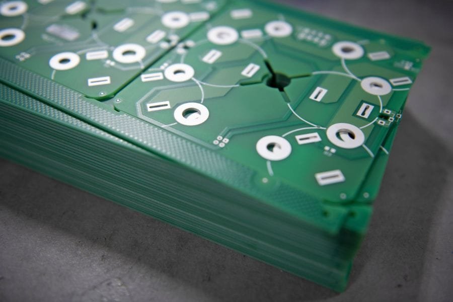
A rigid PCB is a type of Printed Circuit Board that is made from a solid and inflexible material, typically a fiberglass-reinforced plastic material. Unlike flexible PCBs, which are made from flexible materials and can be bent or shaped, rigid PCBs are rigid and cannot be flexed.
Rigid PCBs are used in a wide range of electronic applications, from simple devices such as calculators and cell phones to complex systems such as computers and medical equipment. They are particularly well-suited for high-density applications that require a large number of components to be packed into a small space.
The manufacturing process for rigid PCBs typically involves the application of multiple layers of conductive and insulating materials to a substrate material, followed by the drilling of holes for components and the routing of electrical connections. The finished product is then tested to ensure that it is functioning properly.
Rigid PCBs offer several advantages over flexible PCBs, including greater stability, higher density of components, and improved performance in high-temperature applications. They are also typically more cost-effective to manufacture in large quantities.
What is a Flexible Circuit Board?
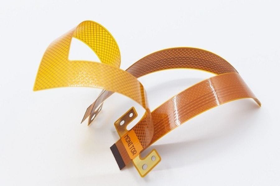
A flexible circuit, also known as a flexible printed circuit board, is a type of circuit that is made from flexible materials, such as polyimide or polyester. Unlike traditional rigid PCBs, which are made from rigid materials and cannot be bent or shaped, flexible circuits are flexible and can be easily integrated into a wide range of electronic devices.
Flexible circuits are used in a variety of applications, including wearable electronics, mobile devices, medical equipment, and automotive electronics. They offer several advantages over traditional rigid PCBs, including improved flexibility, lightweight, and reduced form factor.
The manufacturing process for flexible circuits involves the deposition of conductive and insulating materials onto a flexible substrate, followed by the patterning of the circuit using photolithography and etching techniques. The finished product is then tested to ensure that it is functioning properly.
Flexible circuits offer several advantages over traditional rigid PCBs, including improved reliability, enhanced performance in applications where the circuit is required to bend or flex, and reduced form factor. However, they can be more challenging to manufacture and are typically more expensive than traditional rigid PCBs.
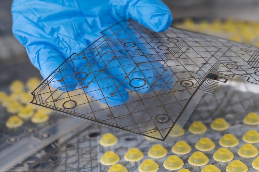
A rigid-flex Printed Circuit Board is a type of circuit that combines the best features of rigid and flexible PCBs. As the name suggests, a rigid-flex PCB is made up of both rigid and flexible components and provides the benefits of both types of circuits.
In a rigid-flex PCB, the rigid components provide the stability and support needed for high-density component placement, while the flexible components allow for the circuit to bend and conform to irregular shapes. This makes rigid-flex PCBs well-suited for applications where both stability and flexibility are required, such as in aerospace and defense, medical devices, and consumer electronics.
The manufacturing process for rigid-flex PCBs involves the deposition of conductive and insulating materials onto both rigid and flexible substrates, followed by the patterning of the circuit using photolithography and etching techniques. The finished product is then tested to ensure that it is functioning properly.
Rigid-flex PCBs offer several advantages over traditional rigid and flexible PCBs, including improved reliability, reduced form factor, and enhanced performance in applications where both stability and flexibility are required. However, they can be more challenging to manufacture and are typically more expensive than traditional rigid or flexible PCBs.
What is the Structure of PCB?
The structure of a PCB typically consists of the following elements:
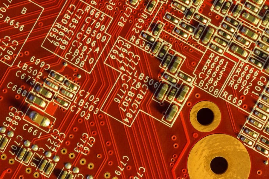
- Copper Traces: The conductive pathways on the surface of the PCB, connecting electronic components.
- Pads: The circular or rectangular areas where electronic components are soldered to the PCB.
- Vias: Small holes drilled through the PCB that allow electrical connections between the different layers of the board.
- Plated Through-Holes (PTH): Holes drilled through the PCB that are filled with metal and provide a connection between the surface and the internal layers of the PCB.
- Solder Mask: A layer of insulating material that covers the surface of the PCB, protecting the copper traces from damage and ensuring the reliability of electrical connections.
- Silkscreen: A layer of ink applied to the surface of the PCB that provides labeling and identification for the components and pathways.
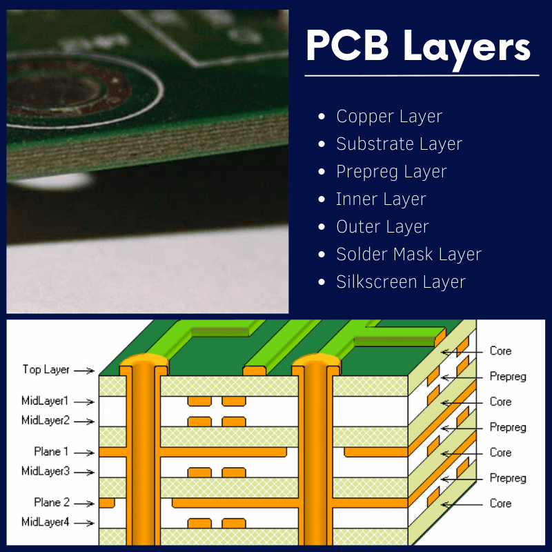
Learn More: PCB Layers Explained:
What are the Materials used for PCB?
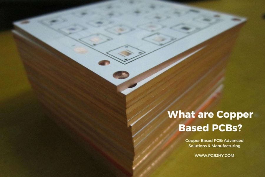
The most commonly used material for PCBs is fiberglass, specifically a material known as FR-4. FR-4 is a fire-resistant and durable material that provides good insulation properties, making it ideal for use in electronic devices.
Other materials that can be used in PCB production include polyimide, polyester, and paper-phenolic.
Learn More: Complete Guide for PCB Material
What is PCB manufacturing?
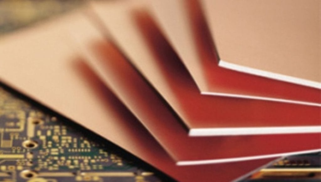
PCB manufacturing refers to the process of creating a Printed Circuit Board from raw materials into a finished, functional product. This process typically involves several steps, including substrate preparation, depositing the conductive material, patterning the conductive material, applying the insulating material, drilling holes, plating the holes, applying the surface finish, component assembly, and testing.
Each of these steps is performed using specialized equipment and materials and requires a high degree of precision to ensure that the finished product meets the desired specifications and will function properly. PCB manufacturing is a complex process that requires experience, skill, and attention to detail to produce a high-quality circuit that meets the desired specifications.
In the PCB manufacturing process, it is important to work with a reputable manufacturer that has the necessary expertise, equipment, and materials to produce a high-quality circuit. The manufacturer should also have a quality control process in place to ensure that each circuit is thoroughly tested and inspected before it is shipped to the customer.
Learn more about our PCB manufacturing services
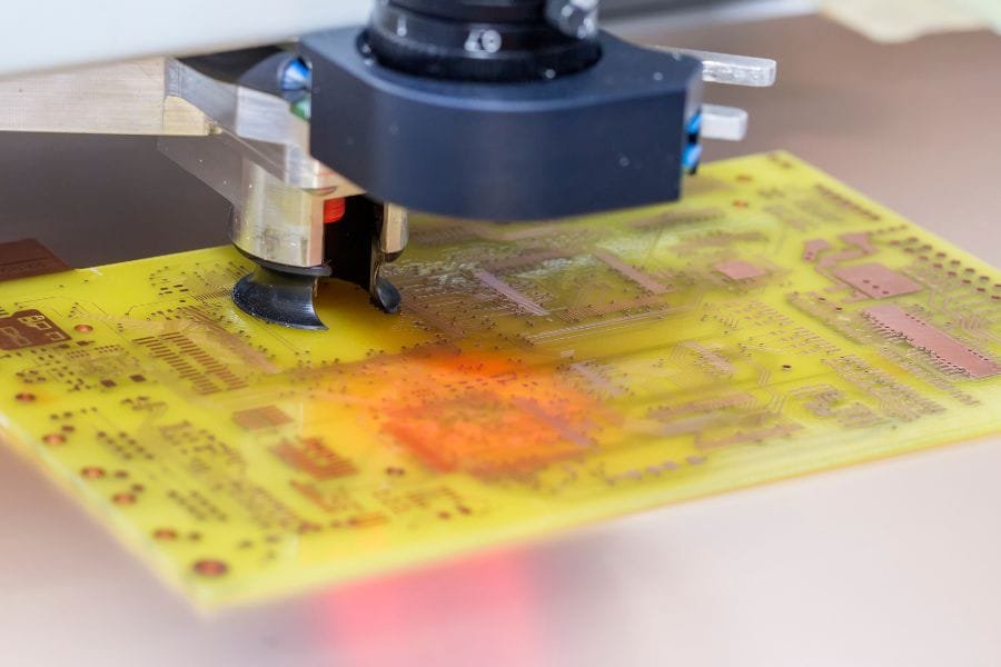
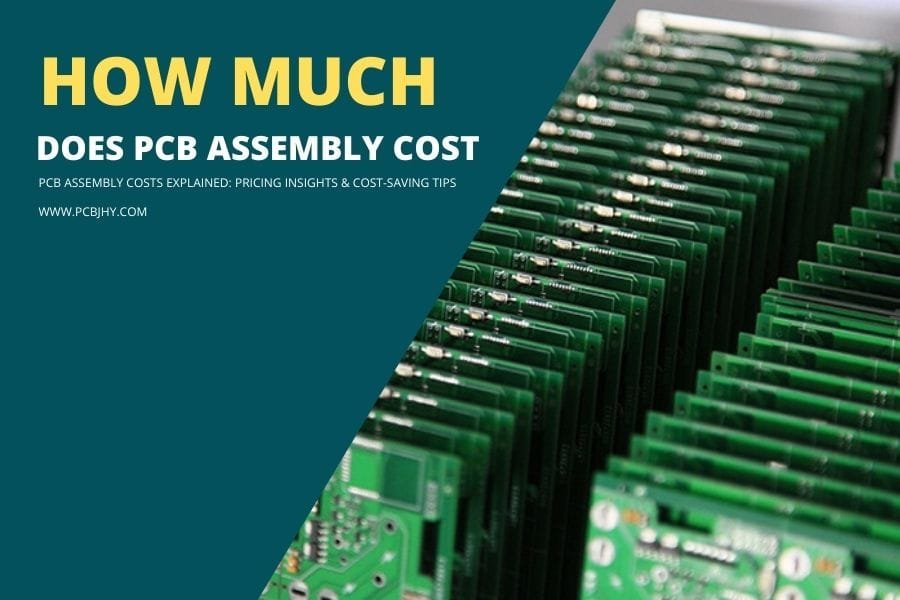
PCB assembly refers to the process of attaching electronic components to a Printed Circuit Board to create a functioning circuit. This process involves several steps, including component placement, soldering, and testing.
- Component placement: The components are physically placed onto the PCB in their designated positions, following the design of the circuit.
- Soldering: The components are soldered onto the PCB to create an electrical connection between the components and the conductive pathways on the PCB. This is typically done using a wave soldering machine or a reflow oven.
- Testing: The finished circuit is tested to verify that it is functioning properly and meets the desired specifications. This may involve power-on testing, functional testing, and in-circuit testing to ensure that all of the connections are properly made and that the circuit is functioning as designed.
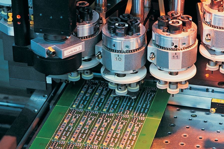
PCB assembly requires a high degree of precision and attention to detail to ensure that the components are properly placed and soldered and that the circuit is functioning properly. This process is typically performed by an experienced assembly technician or by an automated assembly machine. The choice of assembly method will depend on the size and complexity of the circuit, the desired production volume, and the desired level of precision and quality control.
Learn more about our PCB assembly services
How to design a PCB?
The design of a PCB is crucial for ensuring the reliability and functionality of an electronic device. The design process involves several steps, including schematic design, layout design, and fabrication.
In schematic design, the electrical connections between the components are defined. This information is then used in the layout design to determine the placement of components and the routing of the copper traces on the surface of the PCB.
Designing a Printed Circuit Board involves several steps, including the following:
- Define the requirements: Determine the specifications of the circuit, including the number and type of components, the desired form factor, and the desired electrical performance.
- Create a schematic: Create a schematic diagram that represents the electrical connections between the components. This diagram should be used to verify that the circuit will function as desired.
- Select the components: Choose the components that will be used in the circuit and verify that they are compatible with the schematic and the form factor.
- Choose a PCB layout software: Choose a PCB layout software that is compatible with the schematic and the components and that offers the features and tools needed for the desired form factor and electrical performance.
- Layout the PCB: Use the PCB layout software to lay out the components and the electrical connections on the PCB. This should be done with consideration for the routing of the electrical connections, the placement of the components, and the desired form factor.
- Verify the design: Verify that the layout is correct and that the electrical connections are properly routed. Check for any errors or issues that could impact the performance or reliability of the circuit.
- Generate the manufacturing files: Generate the manufacturing files, including the Gerber files and the drill files, that will be used by the PCB manufacturer to create the circuit.
- Manufacture the PCB: Send the manufacturing files to a PCB manufacturer to have the circuit fabricated.
- Test the PCB: Test the finished circuit to ensure that it is functioning properly and meets the desired specifications.
This is a general outline of the steps involved in designing a PCB. The specific steps and tools used may vary depending on the desired form factor, electrical performance, and the components used. It is important to seek the assistance of an experienced PCB designer or to consult a reference guide to ensure that the design is correct and that the finished product will function as desired.
Related Reading:
- A Comprehensive Guide to 8 Layer PCB Stackup Design
- High Speed and High Frequency PCB Design: Similarities and Key Distinctions
- LED PCB Design Guide: Tips and Best Practices for Manufacturers
- Choosing the Right Materials for Your High-Frequency PCB Design
- Multilayer PCB Design Guide: A Comprehensive Overview
- Rigid Flex PCB Design Guidelines: Key Guidelines to Follow
- High Tg PCB Design Guidelines: Best Practices and Tips for Success
- Design Considerations for Metal Core PCBs: Tips and Tricks for Optimal Performance
- How to Calculate Controlled Impedance for PCB Design?
- Understanding Common Controlled Impedance Types in PCB Design
- How to Design a Heavy Copper PCB?
How to Make a PCB?
The process of making a Printed Circuit Board typically involves several steps:
- Design: The first step in making a PCB is to create a design using computer-aided design (CAD) software. This design should include the layout of the circuit, including the placement of components and the routing of electrical connections.
- Preparing the substrate: The substrate, typically made of fiberglass or other materials, is cut to size and the desired number of layers is laminated together to form the base of the PCB.
- Depositing the conductive material: A thin layer of copper is deposited onto the substrate to create the electrical pathways for the circuit.
- Photoplotting: Once the design is complete, a film positive of the circuit pattern is created using photo plotting equipment. This film positive is used to transfer the circuit pattern to a metal plate.
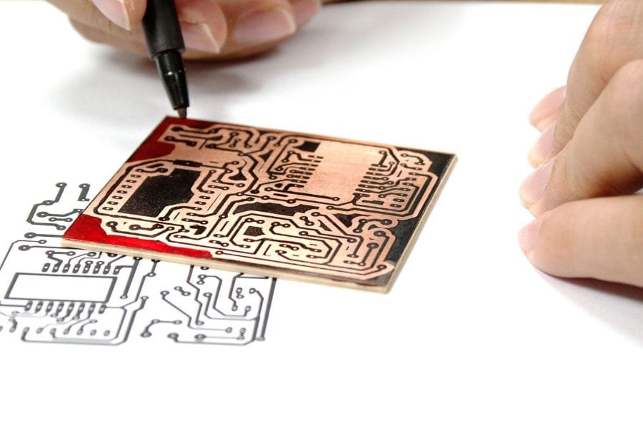
- Etching: The metal plate is then etched, using the film positive as a mask, to remove all of the metal except for the desired circuit pattern.
- Drilling: Holes are drilled in the metal plate where components will be inserted. These holes are used to connect the components to the metal circuit pattern.
- Lamination: A layer of insulating material is added to the metal plate, typically by laminating a layer of epoxy-glass or similar material to the metal.
- Plating: A layer of metal, typically copper, is added to the laminated board to create the final circuit pattern. This is typically done by electroplating the metal onto the surface of the board.
- Finishing: The surface of the board is finished, typically by applying a layer of protective solder mask and silkscreen printing the component designations and other information onto the board.
- Testing: The finished PCB is tested to ensure that it is functioning properly. This can involve a visual inspection, continuity testing, and functional testing.
This is a high-level overview of the PCB manufacturing process. There can be many variations and additional steps involved, depending on the specific requirements of the PCB and the manufacturing process used.
What is the PCB cost?
The cost of a Printed Circuit Board depends on several factors, including:
- The size of the board: Larger boards generally cost more than smaller ones.
- The number of layers: Multilayer boards are more expensive than single-layer boards.
- The complexity of the circuit: More complex circuits require more precise manufacturing processes and can therefore cost more.
- The material used: Different PCB materials have different costs. For example, FR-4 is a commonly used material that is relatively inexpensive, while Rogers material is more expensive but offers better performance.
- The manufacturer: The cost of PCBs can vary depending on the manufacturer and their location.
- The quantity: The cost of PCBs decreases as the quantity ordered increases, due to economies of scale.
It’s also worth noting that the cost of PCBs can vary widely depending on the specific requirements of a project. A precise cost estimate can only be determined by considering all of the relevant factors and obtaining quotes from multiple suppliers.
Related Reading:
- How Much Does a PCB Prototype Cost? Pricing Guide for 2024
- Key Factors Influencing Bare PCB Manufacturing Costs
- How to Reduce PCB Costs Without Sacrificing Quality
- Supply Chain Management: How to Optimize Cost and Delivery Time for PCB Components
- Material selection and performance of multilayer PCBs: how to balance cost and performance
- High Tg PCB Cost and Pricing: Factors Affecting the Price and How to Save Money
What are the benefits of PCB?
Printed Circuit Boards have several benefits, which have made them the preferred choice for many electronic applications:
- Reliability: PCBs are reliable and durable, providing a secure connection between components that lasts for the life of the product.
- Space savings: PCBs allow for a compact design of electronic devices, saving space and making it possible to create smaller, more portable products.
- Efficient routing: PCBs allow for the efficient routing of electrical signals, reducing the risk of electrical interference and improving the performance of the device.
- Improved performance: PCBs allow for better heat dissipation, reducing the risk of component damage and improving the overall performance of the device.
- Cost-effectiveness: PCBs are cost-effective, especially in large quantities, as the cost per board decreases as the quantity ordered increases.
- Repeatability: PCBs can be manufactured repeatedly with consistent results, ensuring that each device is made to the same high standards.
- Automation: The manufacturing process of PCBs can be automated, reducing the risk of human error and improving the consistency and accuracy of the manufacturing process.
- Flexibility: PCBs can be designed in a variety of shapes and sizes, allowing for greater design flexibility and enabling the creation of complex electronic devices.
These benefits have made PCBs an important component in a wide range of electronic devices and systems, and have helped to drive the growth of many industries and technologies.
What are the Printed Circuit Board Applications?
PCBs are used in a wide range of applications due to their ability to securely and efficiently connect electronic components. Some common applications of PCBs include:
- Computers and peripherals: PCBs are used in computer systems, including motherboards, hard drives, and other components.
- Consumer electronics: PCBs are used in a variety of consumer electronics products, including smartphones, televisions, and gaming consoles.
- Medical equipment: PCBs are used in many medical devices, such as heart monitors and blood glucose meters.
- Automotive electronics: PCBs are used in a variety of automotive applications, including engine management systems, safety systems, and entertainment systems.
- Industrial controls: PCBs are used in industrial automation and control systems, including programmable logic controllers (PLCs) and human-machine interfaces (HMIs).
- Military and aerospace: PCBs are used in a wide range of military and aerospace applications, including satellites, aircraft, and defense systems.
- Power electronics: PCBs are used in power electronics applications, such as switch-mode power supplies and motor controls.
- Communication equipment: PCBs are used in communication equipment, including routers, switches, and modems.
These are just a few examples of the many applications of PCBs. The versatility and reliability of PCBs make them an important component in a wide range of industries and products.
How and where to get a PCB?
PCBs can be obtained from a variety of sources, including:
- PCB manufacturers: The most common source for PCBs is a dedicated PCB manufacturer. These companies specialize in the production of PCBs and can offer a wide range of services, from design and prototyping to mass production. Many PCB manufacturers offer online ordering systems and can provide quick turnaround times for smaller orders.
- PCB fabrication houses: PCB fabrication houses are specialized companies that focus solely on the production of PCBs. They may offer a wider range of services, including design support, prototyping, and high-volume production.
- Online PCB suppliers: There are many online PCB suppliers that offer quick and easy ordering of custom PCBs. These suppliers often have streamlined ordering systems and can provide quick turnaround times for smaller orders.
- Electronics distributors: Electronics distributors often carry a wide range of PCBs, including both standard and custom designs. They may also offer design support and prototyping services.
- Local electronics stores: Some local electronics stores may carry a limited selection of PCBs, including prototype boards and pre-made circuit boards.
It is important to choose a reputable source for your PCBs to ensure that you receive a high-quality product that meets your specifications. When selecting a supplier, consider factors such as the company’s experience and reputation, the range of services offered, and the quality of their customer support.
Summary
In conclusion, a Printed Circuit Board is an essential component in the manufacturing of electronic devices. Its design, material, and manufacturing process are critical factors in ensuring the reliability and functionality of the final product. The design of the PCB involves several steps, including schematic design, layout design, and fabrication, and involves the placement of components, the routing of copper traces, and the creation of electrical connections. The material used for the PCB is typically fiberglass, but other materials, such as polyimide and polyester, can also be used. The process of making a PCB involves several steps, including etching, drilling, laminating, and soldering.
In recent years, advancements in technology have led to the development of new PCB materials and manufacturing techniques, such as the use of surface mount technology (SMT) and the implementation of automated manufacturing processes. The use of SMT has made it possible to create smaller and more complex PCBs, leading to the development of more advanced and compact electronic devices.
The importance of PCBs in the manufacturing of electronic devices cannot be overstated. They provide a platform for the creation of complex electronic circuits, ensure the reliability of electrical connections, and provide a means of connecting electronic components. The continued development and improvement of PCB technology will continue to play a crucial role in the advancement of the electronics industry.
JHYPCB: a leading PCB manufacturer in China
Here at JHYPCB, we can offer a full range of PCB manufacturing and assembly services for all types of designs and performance requirements.
With over 10 years of experience in printed circuit board fabrication and assembly, we’ve developed a leading China reputation for both flawlessly accurate technical work, and some of the fastest lead times in the industry.
Our complete PCB solutions:
- PCB Prototyping
- Custom PCB Manufacturing
- Flexible Circuit board Fabrication
- Rigid PCB Fabrication Service
- Rigid-Flex PCB Manufacturing Service
- Metal Core PCB Fabrication Service
- Low-to-High Volume PCB Manufacturing Service
- Prototype PCB Assembly Service
- Turnkey PCB Assembly Service
- Small quantity to High-volume PCB Assembly Service
If you’d like to discuss any aspect of an upcoming PCB production project with a member of our team, please feel free to contact us at sales@pcbjhy.com.
Related Reading
- Multilayer PCB Manufacturer: How to Choose the Right One for Your Project?
- The Importance of Choosing the Right Aluminum PCB Manufacturer
- High Tg PCB Manufacturing: How It Works and What to Look for in a PCB Manufacturer
- How To Choose The Right HDI PCB Manufacturer?
- Key Considerations for Choosing a Reliable Single-Layer PCB Manufacturer

