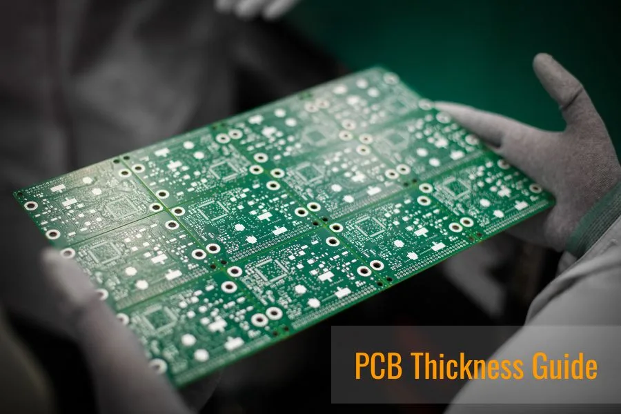
Introduction
Designing printed circuit boards requires carefully selecting the right board thickness for your application. The PCB thickness has a major impact on performance factors like current capacity, impedance control, and mechanical stability.
Choosing the optimal PCB thickness depends on considerations like:
- Layer count – The number of conductive layers affects the overall thickness. A 2-layer board will be thinner than a 12-layer board.
- Copper thickness – The thickness of the copper foil used for traces and pads impacts current capacity and impedance. Thicker copper provides higher ampacity.
- Mechanical requirements – The PCB must be thick enough to provide structural rigidity and durability for the application.
- Flexibility needs – Flex PCBs require very thin, flexible boards to withstand bending and folding.
This comprehensive PCB thickness guide covers all the key information you need to select the right thickness for your next board design. We’ll explain the standard PCB, copper, and trace thicknesses used in fabrication. You’ll learn thickness ranges for flex PCBs versus rigid boards. We’ll also dive into how layer count, current capacity, impedance, manufacturing capabilities, and cost factors into choosing your optimal PCB thickness.
With the help of this guide, you’ll be able to optimize your printed circuit board thickness for electrical performance, mechanical stability, and manufacturability. You’ll avoid common pitfalls like boards that are too thin and prone to damage or overly thick boards that are unnecessary and expensive. Get ready to make informed PCB thickness decisions to ensure your next board design meets your product needs.
Standard PCB Thicknesses
When selecting a PCB thickness, the first step is understanding the standard thickness ranges available for different board materials. FR-4 glass epoxy is the most common rigid PCB material, with a typical thickness between 0.4mm to 1.6mm.
Here are the standard thicknesses available for mainstream PCB materials:
- FR-4 Glass Epoxy: 0.4mm, 0.6mm, 0.8mm, 1.0mm, 1.2mm, 1.6mm
- CEM-1: 0.25mm, 0.4mm, 0.6mm, 0.8mm, 1.0mm
- CEM-3: 0.4mm, 0.6mm, 0.8mm, 1.0mm
- Rogers RO4003: 0.203mm, 0.254mm, 0.305mm, 0.5mm, 0.8mm, 1.0mm
In general, thicker PCBs offer:
- Greater mechanical strength and durability
- Higher current capacity and lower trace resistance
- Better thermal performance for heat dissipation
Thinner boards tend to be lower cost, more flexible, and take up less space. Ultra-thin 0.25mm PCBs are prone to warping and twisting, while boards above 1.6mm are unnecessary for most applications.
When selecting a standard PCB thickness, consider the minimum thickness required for structural rigidity, as well as thermal and electrical constraints. We’ll explore those factors in more detail throughout this guide.
The PCB thickness specified by the customer is the thickness of the board after fabrication is completed.
| Nominal thickness of copper clad laminate | |||||||||||
|---|---|---|---|---|---|---|---|---|---|---|---|
| mm | 0.5 | 0.7 | 0.8 | 1.0 | 1.2 | 1.5 | 1.6 | 2.0 | 2.4 | 3.2 | 6.4 |
| mils | 20 | 28 | 31 | 40 | 47 | 59 | 63 | 79 | 95 | 126 | 252 |
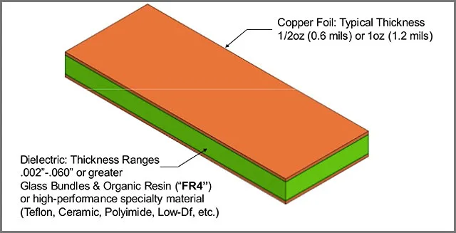
PCB Copper and Trace Thicknesses
The thickness of the copper foil used for traces and pads is another key factor determining PCB thickness and performance. Copper thickness is measured in ounces – the most common weights are 0.5 oz, 1 oz, 2 oz, and 3 oz.
Thicker copper provides:
- Higher current capacity. A 2 oz copper trace can carry over 50% more current than a 1 oz trace.
- Lower electrical resistance. Double the copper thickness halves the resistive losses.
- Better heat dissipation. Thick copper spreads heat more efficiently.
Standard PCB trace thicknesses range from:
- 0.1 mm – Typical for high-density boards
- 0.125 mm – Common for digital circuits
- 0.2 mm – Used for high-current power circuits
Thicker traces withstand higher currents, but take up more space on the PCB. A 0.2mm trace can carry over 3 times more current than a 0.1mm trace with the same temperature rise.
When selecting copper and trace thicknesses, calculate the current levels in your circuit. Choose a copper weight that provides the required current capacity with safe temperature rise. Verify the PCB fabricator can produce the minimum trace width and spacing needed for your design. Optimizing copper and trace thicknesses balances electrical and physical constraints.
Why is the PCB Copper Thickness Unit in Ounces?
The thickness of copper foil used in PCB fabrication is commonly specified in ounces, which refers to the weight of copper per square foot. This unusual unit is a holdover from the early days of printed circuit board manufacturing.
Originally, copper foil was produced in standard 1 oz and 2 oz weights per square foot. As PCBs became more complex, greater precision was needed. So fractional ounce measurements were introduced, with 1/2 oz, 1/3 oz, and even 1/10 oz foils.
Using ounces provides a consistent basis to compare the thickness of different copper foils. Heavier copper foil in ounces equates to a thicker physical layer on the PCB.
While metric units like microns would seem more intuitive, the ounce has remained the standard for historical reasons. It allows continuity with existing PCB manufacturing processes and avoids confusion switching measurement systems.
The conversion between ounces and microns is straightforward:
- 1 oz Cu = 35 μm
- 0.5 oz Cu = 18 μm
- 2 oz Cu = 70 μm
- 3 oz Cu=105 μm
So when you see copper thickness in ounces on PCB datasheets and specifications, you’ll know it refers to the weight per square foot, which directly corresponds to the physical foil thickness in microns. The ounce continues as the standard today for specifying copper amounts in PCB design and fabrication.
Generally, the PCB copper thickness of single-sided and double-sided boards is about 35μm (1.4mil). Other common specifications are 50μm and 70 μm. For multilayer boards, the surface layer copper is generally 35μm=1oz (1.4mil), while the inner layer is usually 17.5 μm (0.7mil).
Note:
1. 1 ounce (oz) = 28.3495 grams
2. 1oz copper thickness refers to 1oz of copper covering the area of 1 square foot uniformly. It is about 1.4mil.
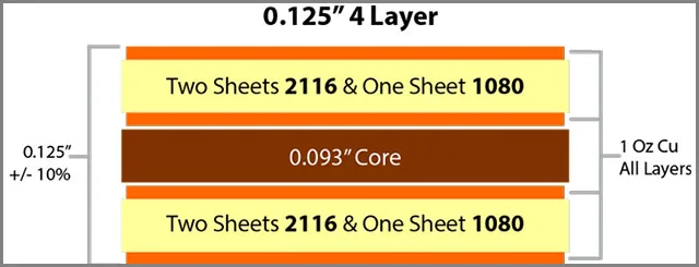
PCB Core Thickness
The core layer or dielectric substrate is the insulating material that separates conductive copper layers in a PCB. For a simple 2-layer board, the single core layer separates the top and bottom copper layers. In multilayer boards, additional core layers are stacked between copper layers.
Common rigid PCB core materials are FR-4, high Tg epoxy, TG130, Rogers, and polyimide. Core thickness is typically standardized based on layer count:
- 2-6 layer boards: 1.6 mm core
- 8-10 layer boards: 1.0 mm core
- 12+ layer boards: 0.8 mm or thinner cores
However, specific electrical or mechanical requirements may necessitate different core thicknesses. For example:
- Thicker 3.2 mm core for increased structural rigidity
- Thinner 0.2 mm core for tightly controlled impedance
In short, while standard thicknesses exist, it’s important to evaluate core thickness based on the individual PCB design needs and fabrication capabilities. Work closely with your PCB manufacturer to determine the optimal core thicknesses.
Pre-Preg Thickness
Pre-preg layers are glass fabric impregnated with resin that are placed between PCB core layers. When pressed together during lamination, the pre-preg layers change thickness unlike the cores. Therefore pre-pregs can be used to modify overall PCB thickness. The resultant pre-preg thickness depends on the fabrication process and the ratio of copper to dielectric areas in each layer. To control overall PCB thickness, work with your manufacturer to select appropriate pre-preg materials and fabrication parameters.
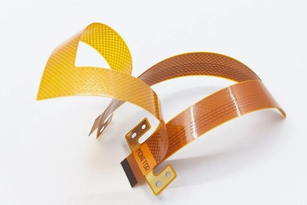
Flex PCB Design Considerations
Flex PCBs provide the ability to bend and fold electronic circuits. To achieve flexibility, flex boards are much thinner than rigid PCBs.
Typical flex PCB thicknesses range from:
- 25 to 50 microns – Ultra-thin flex, allows tight bending
- 50 to 100 microns – Common flexible thickness
- 130 to 200 microns – Approaching rigid-flex thickness
The most common flex PCB constructions are:
- Single layer flex – One conductive layer, simple low-power circuits
- Double layer flex – Allows more complex circuit layouts
- Rigid-flex – Combines multiple rigid PCBs joined by flexible sections
Designing reliable flex PCBs requires managing flexibility and minimizing stresses. Common techniques include:
- Using polyimide instead of FR4 to improve flexure
- Adopting rounded traces instead of angular corners
- Strategic placement of components in rigid areas
Flex PCBs allow creative packaging solutions not possible with rigid boards. However, the specialized materials and processes required make flex PCB fabrication more complex and costly.
Layer Count and Thickness
The number of conductive copper layers in a PCB stackup directly impacts the total board thickness. Here are typical thickness ranges for standard layer counts:
- 2 layer boards – 0.6mm to 1.6mm
- 4 layer boards – 0.8mm to 2.4mm
- 6 layer boards – 1.2mm to 3.2mm
- 8-12 layer boards – 1.6mm to 4.8mm
Increasing layer count allows the routing of complex, high-density PCBs. However, each additional layer adds:
- Fabrication complexity – Hi-tech processes required
- Increased thickness – Additional dielectric and copper add up
- Higher cost – Extra production steps increase expense
High layer counts may require thinner dielectrics to control overall thickness. But dielectrics thinner than 0.1mm become challenging to manufacture.
In high-frequency digital and RF designs, stacking multiple thin dielectrics with tight laminate control reduces signal loss. But the laminating process limits the minimum achievable thickness.
Ensure your PCB fabricator can build the layer count you need within your desired thickness. Consult their capabilities and guidelines when making layer count and thickness decisions.

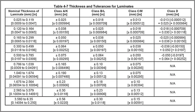
PCB Thickness Tolerance
PCB thickness tolerance refers to the acceptable variance from the nominal thickness value during manufacturing. It is the allowance or deviation from the standard amount of dielectric material that is considered acceptable.
PCB fabricators follow thickness tolerance guidelines provided by the IPC (Association Connecting Electronics Industries). The IPC-6012 specification gives different classes of PCB thickness tolerance based on the layer count:
- Class A: ±10% for layers ≤ 6
- Class B: ±8% for layers 7-14
- Class C: ±6% for layers ≥ 14
So for a nominal 1mm thick, 6-layer board, Class A allows the finished thickness to range from 0.9mm to 1.1mm.
Tighter tolerances are possible but increase manufacturing difficulty and cost. OEMs work with their PCB suppliers to determine appropriate thickness tolerances for each design based on factors like:
- Layer count
- Material selection
- Fabrication capabilities
- Electrical, thermal and mechanical requirements
Properly specifying thickness tolerance gives the fabricator needed latitude while ensuring the completed boards function as intended. Optimizing tolerance relative to application needs balances quality and cost.
Key Factors in PCB Thickness Selection
Let’s summarize the key considerations when selecting an optimal PCB thickness:
Mechanical Stability:
- The PCB must be thick enough to provide sufficient physical rigidity and resistance to shock/vibration.
- Thinner boards are prone to warping which can fracture traces.
- For handheld devices, 1.6mm or thicker is recommended.
Current Carrying Capacity:
- Thicker copper provides higher current capacity based on: I=kΔTA/R
- Increase copper thickness or widen traces to handle required current levels.
Impedance Control:
- Match target impedance Zo using: Zo= (L/C)1/2
- Adjust dielectric thickness and trace dimensions to tune impedance.
Manufacturing Capability:
- Confirm PCB fabricator can produce designed layer count and thickness.
- Thinner dielectrics and tighter tolerances increase cost.
Thermal Management:
- Thicker copper helps spread heat, but thicker dielectric reduces heat transfer.
- Use thermal vias and thicker outer layers for cooling.
Consider all these factors together to optimize PCB thickness for an effective design.
Material Selection Considerations
The dielectric material used in PCB fabrication also impacts the design process and optimal thickness selection. Key material properties to consider include:
Thermal Conductivity:
- Materials like FR-4 epoxy have lower thermal conduction, limiting heat transfer.
- This may require thicker dielectric for desired insulation or thinner layers to dissipate heat.
Dielectric Constant (Dk):
- Dk affects signal propagation speed and impedance.
- High performance materials like PTFE have lower Dk to minimize signal loss.
Coefficient of Thermal Expansion (CTE):
- CTE determines thermal expansion under temperature changes.
- Matching copper and dielectric CTE reduces thermal stresses.
Frequency Range:
- FR-4 is suitable up to a few GHz, while exotic materials can reach >100 GHz.
- High frequency materials are more tightly controlled for best performance.
Cost:
- Base materials like FR-4 provide the most cost-effective solution.
- High frequency materials can be 10-100X more expensive.
Evaluate intended application requirements and select PCB materials accordingly. Consulting with your fabricator early in the design process is recommended.
Conclusion
This guide has provided an in-depth look at the key considerations when selecting a PCB thickness for your application, including:
- Standard thickness ranges for common rigid and flexible PCB materials
- How copper and trace thicknesses affect current capacity and resistance
- Typical layer counts and thicknesses for multilayer boards
- Important factors like mechanical stability, impedance control, and manufacturability
Armed with these guidelines, you can evaluate the electrical, thermal, and mechanical requirements for your PCB. Determine the optimal board and copper thicknesses needed to meet design rules and fabrication capabilities.
Properly optimizing PCB thickness will result in a board that meets your functional needs with adequate structural rigidity. Avoid unnecessary thickness which only adds cost. At the same time, prevent issues like overheating or board flexure by specifying appropriate minimum thicknesses.
With the knowledge provided in this guide, you can make informed PCB thickness selections tailored precisely to your next project requirements. This will streamline the design process, minimize prototyping iterations, and accelerate bringing your product to market.
Related Reading