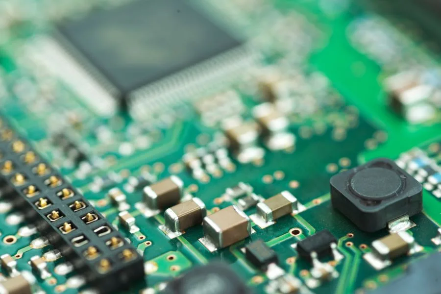
Printed Circuit Boards (PCBs) are the backbone of modern electronic devices. From the simplest gadgets to the most complex machinery, PCBs provide the essential foundation for electrical connections and functionality. Understanding the different types of PCBs is crucial for anyone involved in electronics design, manufacturing, or repair. This knowledge not only helps in selecting the right PCB for your project but also ensures optimal performance and cost-efficiency.
In this comprehensive guide, we will explore the various types of PCBs available today. We will classify them based on several criteria, including the number of layers, flexibility, material composition, application, functionality, and production volume. By the end of this article, you will have a thorough understanding of each PCB type, their unique characteristics, and their specific applications.
Whether you are a seasoned engineer, a hobbyist, or a business looking to optimize your electronics production, this guide is designed to provide valuable insights. Our aim is to help you make informed decisions when choosing the right PCB for your needs.
Stay with us as we delve into the world of PCBs and discover the diverse range of options available. This journey will not only enhance your technical knowledge but also empower you to achieve greater efficiency and innovation in your projects.
Classification by Layers
Printed Circuit Boards can be classified based on the number of layers they contain. This classification is fundamental as it directly impacts the complexity, functionality, and cost of the PCB. Understanding the different layer configurations helps in selecting the right type for specific applications, ensuring the balance between performance and budget. In this section, we will explore single-sided, double-sided, and multi-layer PCBs, examining their unique characteristics and common uses.
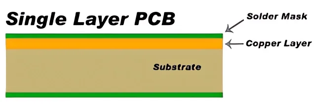
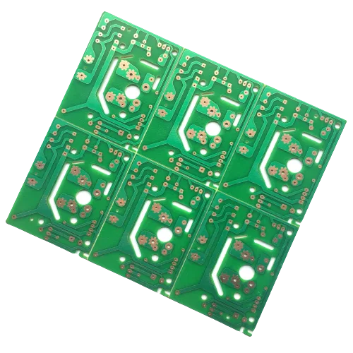
Single-Sided PCBs
Single-sided PCBs, also known as single-layer PCBs, are the most basic type of printed circuit boards. As the name suggests, these PCBs have only one layer of conductive material, typically copper, on one side of the board. The components are mounted on the other side.
Characteristics of Single-Sided PCBs
- Simple Design: Single-sided PCBs have a straightforward design, making them easy to manufacture and suitable for simple, low-density circuits.
- Cost-Effective: Due to their simplicity, they are the most cost-effective option among PCBs. They require fewer materials and less manufacturing time.
- Limited Connectivity: The single layer of conductive material restricts the complexity of the circuits that can be designed. This limitation makes them unsuitable for complex applications requiring multiple connections and higher performance.
Common Applications of Single-Sided PCBs
Single-sided PCBs are widely used in applications where low cost and simplicity are key factors. Some typical applications include:
- Consumer Electronics: Remote controls, calculators, and toys often use single-sided PCBs due to their cost-effectiveness.
- Lighting: Many LED lighting systems use single-sided PCBs, as they do not require complex circuitry.
- Household Appliances: Basic appliances like coffee makers, washing machines, and microwave ovens utilize single-sided PCBs.
Advantages and Disadvantages of Single-Sided PCBs
Advantages:
- Low Cost: Their simple design makes them the cheapest option for PCB manufacturing.
- Easy to Produce: Manufacturing processes for single-sided PCBs are less complex, resulting in faster production times.
- Simplicity: Ideal for simple, low-density applications where advanced features are not necessary.
Disadvantages:
- Limited Functionality: The single layer limits the circuit’s complexity and performance.
- Size Constraints: To accommodate more components, the board size must increase, which can be impractical for compact designs.
- Less Versatile: Not suitable for applications requiring high speed, high frequency, or advanced functionality.
Single-sided PCBs are a great starting point for simple electronic devices. Their cost-effectiveness and ease of manufacturing make them an ideal choice for many basic applications. However, as the need for more complex and higher-performing circuits grows, designers often turn to double-sided or multi-layer PCBs, which we will discuss in the next sections.
Related Reading:
- How Single-Sided PCBs are Made: An In-Depth Look into the Manufacturing Process
- Key Considerations for Choosing a Reliable Single-Layer PCB Manufacturer
- How To Tell single layer PCB From double-sided PCB?
- What are the Single Layer PCB Types?
- How Single-Sided PCBs are Made: An In-Depth Look into the Manufacturing Process
- Key Considerations for Choosing a Reliable Single-Layer PCB Manufacturer
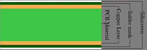
Double-Sided PCBs
Double-sided PCBs, also known as double-layer PCBs, are a step up in complexity and functionality from single-sided PCBs. These PCBs have conductive material, typically copper, on both sides of the board, allowing for more complex and higher-density circuit designs.
Characteristics of Doble-Sided PCBs
- Dual-Sided Conductivity: With copper layers on both sides, double-sided PCBs can accommodate more components and connections than single-sided PCBs.
- Through-Hole Technology (THT): This method involves drilling holes through the PCB, allowing components to be connected through both sides. This increases the board’s connectivity and functionality.
- Surface Mount Technology (SMT): In addition to THT, SMT is often used on double-sided PCBs. Components are mounted directly onto the surface of the PCB, enabling more compact and complex designs.
Common Applications of Double-Sided PCBs
Double-sided PCBs are used in a wide range of applications that require moderate complexity and connectivity. Typical uses include:
- Industrial Controls: Automation systems and machinery control units often utilize double-sided PCBs for their reliability and capability to handle moderate complexity.
- Power Supplies: Power supply units, including adapters and converters, commonly use double-sided PCBs to manage higher power levels and more complex circuitry.
- Consumer Electronics: Devices such as smartphones, audio equipment, and home entertainment systems benefit from the enhanced capabilities of double-sided PCBs.
Advantages and Disadvantages of Double-Sided PCBs
Advantages:
- Increased Connectivity: The ability to have components and connections on both sides of the PCB significantly enhances circuit complexity and performance.
- Compact Design: Double-sided PCBs allow for more components in a smaller area, making them suitable for compact and portable devices.
- Improved Functionality: The combination of THT and SMT provides greater flexibility in design and functionality.
Disadvantages:
- Higher Cost: Manufacturing double-sided PCBs is more complex and expensive compared to single-sided PCBs.
- More Complex Production: The dual-sided nature requires more advanced manufacturing techniques and quality control, which can increase production time and cost.
- Design Complexity: Designing double-sided PCBs requires careful planning and expertise to ensure reliable performance and avoid issues like signal interference.
Double-sided PCBs strike a balance between cost and functionality, making them a popular choice for a variety of electronic applications. Their ability to support more complex circuits than single-sided PCBs while remaining cost-effective makes them ideal for many industrial and consumer products. In the next section, we will explore multi-layer PCBs, which offer even greater capabilities for advanced electronic designs.
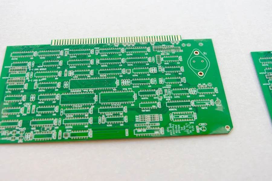
Multi-Layer PCBs
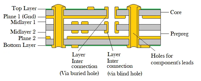
Multi-layer PCBs are the most advanced type of PCBs, consisting of three or more layers of conductive material separated by insulating layers. These PCBs are designed to meet the needs of complex and high-performance electronic applications.
Characteristics of Multi-Layer PCBs
- Multiple Layers: Multi-layer PCBs have several layers of conductive material, which allows for intricate and high-density circuit designs. The layers are laminated together under high pressure and temperature, ensuring a compact and robust structure.
- Enhanced Connectivity: The additional layers provide more routing options for signals and power, reducing the need for long traces and enhancing signal integrity.
- Complex Design: The design of multi-layer PCBs involves careful planning to manage issues such as signal interference, heat dissipation, and layer alignment.
Common Applications of Multi-Layer PCBs
Multi-layer PCBs are used in applications that require high performance, reliability, and compact design. Typical uses include:
- Computers and Servers: Motherboards, graphics cards, and other critical components benefit from the high-density and complex designs of multi-layer PCBs.
- Telecommunications: Networking equipment, including routers, switches, and communication satellites, often use multi-layer PCBs to handle high-speed data transmission.
- Medical Devices: Advanced medical equipment, such as MRI machines and heart monitors, rely on multi-layer PCBs for their critical performance and reliability.
- Aerospace and Defense: Avionics, radar systems, and other high-reliability applications in the aerospace and defense sectors use multi-layer PCBs to meet stringent performance standards.
Advantages and Disadvantages of Multi-Layer PCBs
Advantages:
- High Density: Multi-layer PCBs allow for very complex and dense circuit designs, enabling more functionality in smaller form factors.
- Improved Performance: The additional layers provide better signal integrity, reduced interference, and enhanced power distribution.
- Compact and Lightweight: Multi-layer PCBs support miniaturization, which is essential for modern electronic devices that need to be compact and lightweight.
Disadvantages:
- Higher Cost: The manufacturing process for multi-layer PCBs is more complex and expensive, requiring advanced technology and materials.
- Increased Design Time: Designing multi-layer PCBs is more time-consuming and requires specialized expertise to ensure optimal performance and reliability.
- Complex Manufacturing: The fabrication process involves precise layer alignment, advanced lamination techniques, and stringent quality control, increasing production time and cost.
Multi-layer PCBs are essential for modern electronics that demand high performance and compact designs. Their ability to support complex circuits and provide enhanced connectivity makes them ideal for high-tech applications across various industries. In the following sections, we will explore other types of PCBs classified by flexibility, material composition, and functionality.

Related Reading:
- Choosing the Right 8 Layer PCB Manufacturer for Your Project
- A Comprehensive Guide to 8 Layer PCB Stackup Design
- Multilayer PCB Manufacturer: How to Choose the Right One for Your Project?
- Material selection and performance of multilayer PCBs: how to balance cost and performance
- Multilayer PCB Design Guide: A Comprehensive Overview
- What Are The Benefits And Applications of Multilayer PCB?
- A Guide to Multilayer PCB Manufacturing Process
- PCB Layers Explained: Multilayer PCB Stakcup
Classification by Flexibility
Printed Circuit Boards can also be classified based on their flexibility. This classification is crucial as it determines the board’s suitability for different applications, especially those requiring specific mechanical properties. In this section, we will explore rigid PCBs, flexible PCBs, and rigid-flex PCBs, highlighting their unique characteristics, advantages, and common applications.
Rigid PCBs
Rigid PCBs are the most traditional and widely used type of printed circuit boards. As the name suggests, these boards are made from a solid, inflexible substrate, typically FR-4 (a composite material made of woven fiberglass cloth with an epoxy resin binder that is flame resistant).
Characteristics of Rigid PCBs
- Solid Structure: Rigid PCBs are characterized by their firm and stable structure, which provides a durable base for mounting and connecting electronic components.
- Layered Construction: They can be single-sided, double-sided, or multi-layered, offering various levels of complexity and functionality depending on the application’s requirements.
- Material Durability: The FR-4 material used in rigid PCBs is known for its excellent mechanical strength, insulating properties, and resistance to moisture and high temperatures.
Common Applications of Rigid PCBs
Rigid PCBs are used in a wide range of applications due to their stability and reliability. Some typical uses include:
- Consumer Electronics: Smartphones, tablets, laptops, and desktop computers commonly use rigid PCBs for their internal circuitry.
- Industrial Equipment: Machinery controls, robotics, and automation systems benefit from the robustness and durability of rigid PCBs.
- Automotive Electronics: Car infotainment systems, engine control units, and various sensors rely on rigid PCBs for stable and reliable performance.
- Medical Devices: Diagnostic and monitoring equipment, such as MRI machines and X-ray machines, use rigid PCBs for their critical electronic functions.
Advantages and Disadvantages of Rigid PCBs
Advantages:
- Durability: The solid structure of rigid PCBs provides mechanical stability, making them suitable for applications requiring long-term reliability.
- Cost-Effective: For many standard applications, rigid PCBs offer a cost-effective solution due to their relatively simple manufacturing process and widespread availability.
- High Density: Rigid PCBs can support complex, multi-layer designs, allowing for high-density circuitry and advanced functionality.
Disadvantages:
- Lack of Flexibility: The rigid nature of these PCBs makes them unsuitable for applications where bending or flexing is required.
- Space Constraints: In designs where space is limited and complex shapes are needed, rigid PCBs may not be the best fit.
- Weight: Compared to flexible PCBs, rigid PCBs can be heavier, which might be a consideration in weight-sensitive applications.
Rigid PCBs are a fundamental component of modern electronics, offering a reliable and cost-effective solution for a variety of applications. Their solid structure and ability to support complex circuitry make them indispensable in many industries. Next, we will look into flexible PCBs, which provide an alternative for applications requiring flexibility and adaptability.
Related Reading:
- Why is copper used in PCB?
- The Rainbow of PCBs: A Guide to Solder Mask Colors and Their Uses
- PCB Thickness Guide – Everything You Need to Know for Your PCB Design
- A Complete Guide to HS Codes For PCB & PCBA for Imports and Exports
- Key Factors Influencing Bare PCB Manufacturing Costs
- Rigid PCB Reliability Testing: Methods and Optimization for Stable Performance
- Exploring the Wide Range of Applications for Rigid PCBs
- Exploring and Optimizing Electrical Performance of Rigid PCBs
- Rigid PCB vs. Flexible PCB: Which is Right for Your Next Project?
Flexible PCBs
Flexible PCBs, also known as flex PCBs, are designed to be bent, twisted, and folded into various shapes, making them ideal for applications where space constraints and flexibility are crucial. These PCBs are made from flexible substrates like polyimide, which provide the necessary durability and flexibility.
Characteristics of Flexible PCBs
- Flexible Structure: Flexible PCBs can bend and conform to different shapes, making them suitable for compact and complex electronic designs.
- Lightweight: The materials used in flex PCBs are lighter than those in rigid PCBs, which is beneficial in applications where weight is a concern.
- Durable Materials: Polyimide and other flexible substrates offer excellent resistance to heat, chemicals, and moisture, ensuring reliability in various environments.
Common Applications of Flexible PCBs
Flexible PCBs are used in a wide range of applications where flexibility, weight, and space savings are critical. Some typical uses include:
- Wearable Electronics: Smartwatches, fitness trackers, and other wearable devices benefit from the lightweight and flexible nature of flex PCBs.
- Medical Devices: Flexible PCBs are used in medical implants, portable diagnostic devices, and flexible sensors due to their adaptability and reliability.
- Automotive Electronics: Modern vehicles use flexible PCBs in airbags, antilock brakes, and navigation systems, where the ability to withstand movement and vibration is essential.
- Consumer Electronics: Flex PCBs are found in cameras, smartphones, and foldable devices, providing the necessary flexibility to fit into compact spaces.
Advantages and Disadvantages of Flexible PCBs
Advantages:
- Space Efficiency: Flexible PCBs can be designed to fit into tight and irregular spaces, making them ideal for compact devices.
- Weight Reduction: The lightweight materials used in flex PCBs contribute to overall weight reduction, which is important in portable and wearable devices.
- Durability: Flexible PCBs are resistant to vibrations and mechanical stress, ensuring longevity and reliability in demanding applications.
- Dynamic Flexibility: They can endure repeated bending and flexing, making them suitable for applications with moving parts.
Disadvantages:
- Higher Cost: The materials and manufacturing processes for flexible PCBs are generally more expensive than those for rigid PCBs.
- Complex Manufacturing: Producing flex PCBs requires specialized equipment and techniques, which can increase production time and cost.
- Design Challenges: Designing flexible PCBs requires careful consideration of bend radius, dynamic flexing, and other mechanical factors to prevent damage and ensure reliability.
Flexible PCBs offer unique advantages for applications that require bending, lightweight, and compact designs. Their ability to conform to various shapes and endure mechanical stress makes them invaluable in modern electronics. In the next section, we will explore rigid-flex PCBs, which combine the best features of both rigid and flexible PCBs to offer even greater versatility.

Related Posts:
- Flexible PCB Pricing: Factors, Trends, and Cost-Saving Strategies
- PET vs. PI: the Differences Between these Materials for Flex PCBs
- The Ultimate Guide to Flex PCB Stiffener
- Comprehensive Guide to Manufacturing Flex PCB with Stiffener
- What are the Different Types of Flexible Circuits?
- Unlocking the Versatility of Flex Circuit Design: Applications and Benefits
- What are the Materials for Flex Circuits?
- Flexible PCBs: Advantages And Disadvantages
- Introduction to Rigid Flex PCB Materials
Rigid-Flex PCBs
Rigid-flex PCBs combine the best features of both rigid and flexible PCBs, providing a versatile solution for complex electronic designs. These PCBs consist of multiple layers of rigid and flexible substrates laminated together into a single structure. This hybrid design allows for greater flexibility in design and application, making rigid-flex PCBs ideal for a wide range of advanced electronic devices.
Characteristics of Rigid-Flex PCBs
- Hybrid Structure: Rigid-flex PCBs incorporate both rigid and flexible layers, allowing parts of the board to remain solid and stable while other sections can bend and flex.
- Compact Design: By integrating flexible and rigid sections, rigid-flex PCBs can reduce the overall footprint of the device, leading to more compact and efficient designs.
- Durability: The combination of rigid and flexible materials provides a robust solution that can withstand mechanical stresses, vibrations, and harsh environmental conditions.
Common Applications of Rigid-Flex PCBs
Rigid-flex PCBs are used in advanced applications that require high reliability, compact size, and flexibility. Some typical uses include:
- Aerospace and Defense: Rigid-flex PCBs are used in avionics, missile guidance systems, and other critical aerospace applications where reliability and durability are paramount.
- Medical Devices: Advanced medical equipment, such as pacemakers, hearing aids, and diagnostic imaging systems, utilize rigid-flex PCBs for their compact and reliable designs.
- Consumer Electronics: High-end smartphones, cameras, and laptops often use rigid-flex PCBs to achieve thinner and more compact designs without sacrificing performance.
- Automotive Electronics: Modern vehicles use rigid-flex PCBs in complex systems like navigation, infotainment, and advanced driver-assistance systems (ADAS).
Advantages and Disadvantages of Rigid-Flex PCBs
Advantages:
- Design Flexibility: The combination of rigid and flexible layers allows for innovative designs that can fit into unconventional shapes and spaces.
- Reliability: Rigid-flex PCBs offer enhanced durability and can withstand mechanical stress, making them suitable for high-reliability applications.
- Reduced Connectors: The integration of rigid and flexible sections reduces the need for connectors and cables, improving signal integrity and reducing potential points of failure.
- Space and Weight Savings: By combining rigid and flexible areas, these PCBs can reduce the overall size and weight of the device, which is crucial for portable and compact applications.
Disadvantages:
- Higher Cost: The manufacturing process for rigid-flex PCBs is more complex and costly than that for traditional rigid or flexible PCBs.
- Complex Design and Manufacturing: Designing rigid-flex PCBs requires careful planning and expertise to ensure that both the rigid and flexible sections perform optimally. The manufacturing process also involves multiple steps and precise control, increasing production time and cost.
- Limited Availability: Not all PCB manufacturers have the capability to produce rigid-flex PCBs, which can limit sourcing options and increase lead times.
Rigid-flex PCBs offer a unique combination of flexibility, durability, and compactness, making them ideal for sophisticated electronic devices that require high performance and reliability. Their hybrid nature allows designers to create innovative solutions that would be difficult or impossible with only rigid or flexible PCBs. In the next sections, we will explore other types of PCBs classified by material composition and functionality.

Related Posts:
- What are the Benefits and Advantages of Rigid-Flex PCB?
- Introduction to Rigid Flex PCB Materials
- How to Reduce Manufacturing Costs for Rigid-Flex PCBs?
- A Comprehensive Guide to Rigid Flex PCB Fabrication & Manufacturing Process
- Rigid Flex PCB Design Guidelines: Key Guidelines to Follow
- The Versatility and Applications of Rigid-Flex PCBs
Classification by Material Composition
Printed Circuit Boards can also be classified based on the materials used in their construction. The choice of materials affects the board’s electrical performance, thermal management, durability, and overall cost. In this section, we will explore different types of PCBs classified by their material composition, including FR-4 PCBs, metal core PCBs, and aluminum PCBs. Understanding these material differences is crucial for selecting the right PCB for your specific application needs.
FR-4 PCBs
FR-4 PCBs are the most common type of PCBs used in the electronics industry. FR-4 stands for “Flame Retardant 4,” a grade designation for the glass-reinforced epoxy laminate material used in these boards. The FR-4 material offers a good balance of performance, cost, and durability, making it the standard choice for many electronic applications.
Characteristics of FR-4 PCBs
- Glass-Reinforced Epoxy Laminate: FR-4 is made from woven fiberglass cloth with an epoxy resin binder that is flame resistant, providing a robust and stable substrate for PCBs.
- High Dielectric Strength: FR-4 material offers excellent insulation properties, which is critical for maintaining signal integrity and preventing electrical interference.
- Mechanical Strength: The glass-reinforced nature of FR-4 provides significant mechanical strength, making the boards durable and resistant to bending and warping.
- Thermal Resistance: FR-4 has good thermal resistance, making it suitable for applications where moderate heat dissipation is required.
Common Applications of FR-4 PCBs
FR-4 PCBs are used in a vast array of electronic devices due to their versatility and reliability. Some common applications include:
- Consumer Electronics: Devices such as smartphones, tablets, computers, and televisions widely use FR-4 PCBs.
- Industrial Equipment: Automation systems, control panels, and machinery often incorporate FR-4 PCBs due to their durability and cost-effectiveness.
- Telecommunications: Routers, modems, and other communication devices benefit from the electrical insulation and stability provided by FR-4 PCBs.
- Automotive Electronics: Many electronic components in cars, such as infotainment systems and engine control units, use FR-4 PCBs.
Advantages and Disadvantages of FR-4 PCBs
Advantages:
- Cost-Effective: FR-4 PCBs are relatively inexpensive to produce, making them an economical choice for many applications.
- Versatile: The material properties of FR-4 make it suitable for a wide range of applications, from simple consumer electronics to more complex industrial equipment.
- Durable: The mechanical strength and thermal resistance of FR-4 ensure long-lasting performance in various environments.
- Good Electrical Insulation: High dielectric strength ensures that FR-4 PCBs maintain signal integrity and prevent electrical interference.
Disadvantages:
- Moderate Thermal Conductivity: While FR-4 offers good thermal resistance, it may not be suitable for high-power applications requiring superior heat dissipation.
- Limited High-Frequency Performance: FR-4 materials may not perform optimally in very high-frequency applications where advanced signal integrity is critical.
- Environmental Concerns: The manufacturing process and materials used in FR-4 PCBs can have environmental impacts, requiring proper disposal and recycling methods.
FR-4 PCBs remain the industry standard for many applications due to their balance of performance, durability, and cost. They provide a reliable solution for a wide range of electronic devices, ensuring stable and long-lasting operation. In the next section, we will discuss metal core PCBs, which offer enhanced thermal management for high-power applications.
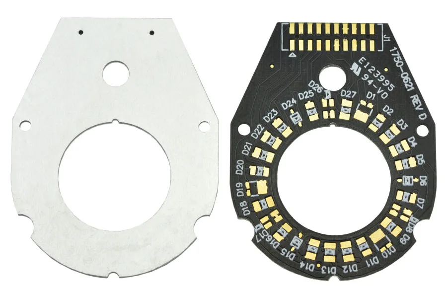
Metal Core PCBs
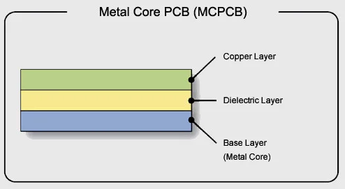
Metal Core PCBs (MCPCBs), also known as thermal PCBs, are designed to improve heat dissipation and manage thermal performance in high-power applications. Unlike traditional PCBs that use FR-4 as the substrate, MCPCBs incorporate a metal core, usually aluminum, copper, or a combination of metal alloys, to provide enhanced thermal conductivity.
Characteristics of Meta Core PCBs
- Metal Core: The core of MCPCBs is typically made of aluminum or copper, which provides excellent thermal conductivity. This core is sandwiched between layers of non-conductive material to insulate and support the circuit.
- Thermal Management: MCPCBs are specifically designed to dissipate heat away from critical components, protecting them from overheating and ensuring stable performance.
- Structural Stability: The metal core adds mechanical strength to the PCB, making it more robust and resistant to mechanical stress and vibration.
Common Applications of Metal Core PCBs
MCPCBs are ideal for applications where heat dissipation is a critical concern. Some typical uses include:
- LED Lighting: High-power LED lights generate significant heat, which MCPCBs can effectively manage, prolonging the lifespan and performance of the LEDs.
- Power Supplies: Power converters, inverters, and other power supply units benefit from the thermal management provided by MCPCBs.
- Automotive Electronics: Headlights, power modules, and engine control systems in modern vehicles use MCPCBs to handle the heat generated by high-power components.
- Telecommunications: High-frequency and high-power communication devices, such as base stations and RF amplifiers, use MCPCBs to maintain signal integrity and performance under thermal stress.
Advantages and Disadvantages of Metal Core PCBs
Advantages:
- Superior Thermal Conductivity: The metal core efficiently conducts heat away from high-power components, reducing the risk of overheating and improving overall performance.
- Enhanced Durability: The metal core provides mechanical strength and stability, making MCPCBs more resistant to physical stress and vibration.
- Improved Performance: Effective thermal management ensures that electronic components operate within optimal temperature ranges, enhancing reliability and longevity.
Disadvantages:
- Higher Cost: The materials and manufacturing processes for MCPCBs are more expensive than traditional PCBs, which can increase the overall cost of the final product.
- Complex Manufacturing: Producing MCPCBs requires specialized equipment and techniques, which can increase production time and complexity.
- Limited Flexibility: The rigid nature of the metal core limits the flexibility of MCPCBs, making them unsuitable for applications requiring flexible or dynamic movement.
Metal Core PCBs are essential for high-power applications where efficient heat dissipation is crucial. Their superior thermal conductivity and structural stability make them an excellent choice for LED lighting, automotive electronics, power supplies, and telecommunications. In the next section, we will explore aluminum PCBs, a specific type of metal core PCB known for its excellent thermal management properties.
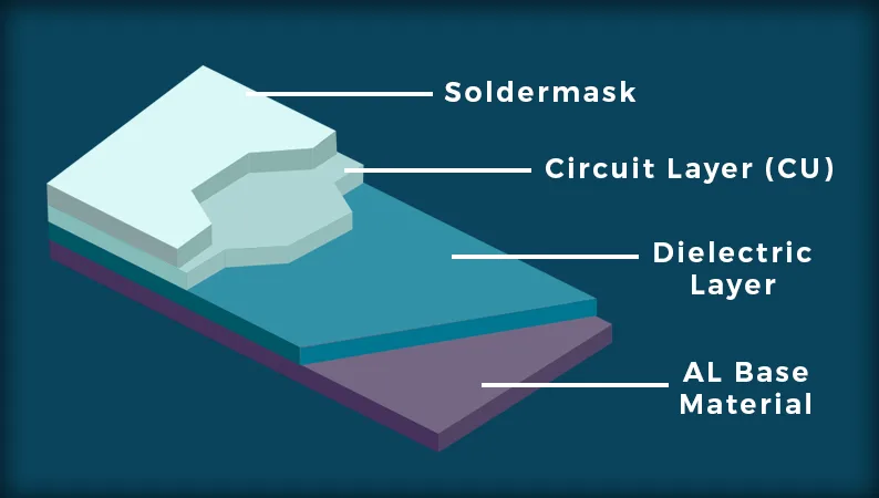
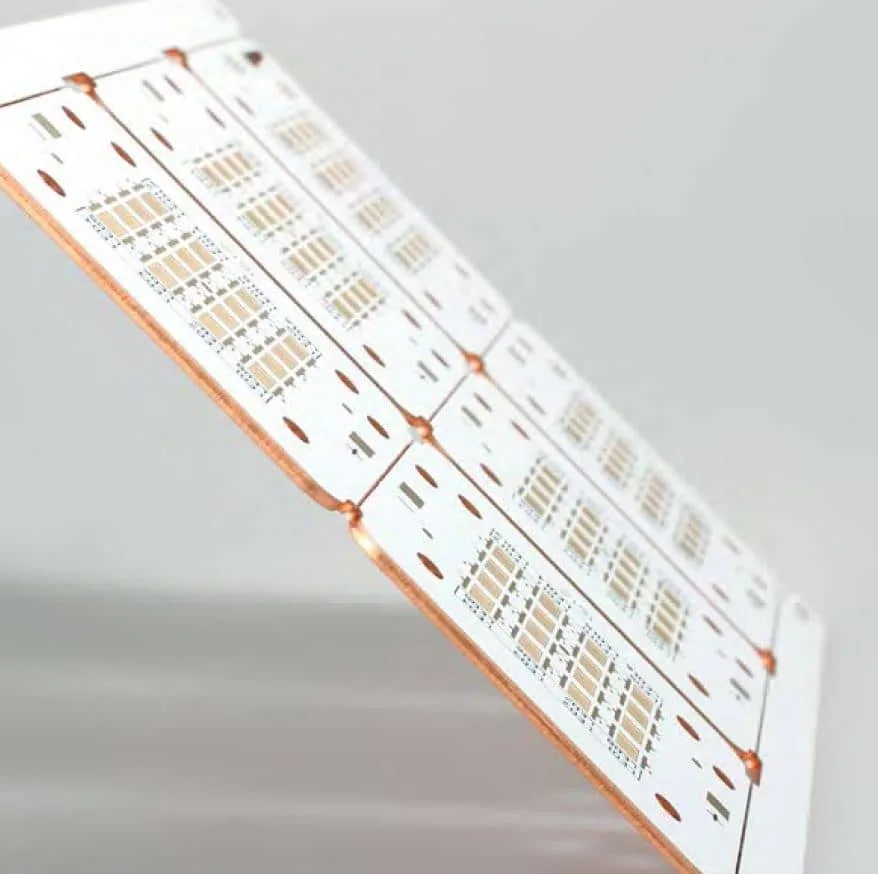
Aluminum PCBs
Aluminum PCBs are a type of metal core PCB that specifically uses an aluminum substrate to enhance thermal management. Known for their excellent heat dissipation properties, aluminum PCBs are widely used in applications where efficient thermal control is critical.
Characteristics of Aluminum PCBs
- Aluminum Core: The core of aluminum PCBs is made from aluminum, which offers superior thermal conductivity compared to traditional FR-4 substrates. This core is typically bonded with a dielectric layer that insulates and separates the electrical circuits from the metal base.
- Heat Dissipation: Aluminum’s high thermal conductivity allows it to effectively transfer heat away from heat-generating components, preventing overheating and ensuring stable performance.
- Lightweight and Durable: Aluminum is a lightweight material, providing structural stability without adding significant weight. This makes aluminum PCBs both durable and suitable for applications where weight is a concern.
Common Applications of Aluminum PCBs
Aluminum PCBs are ideal for applications that require efficient thermal management. Some typical uses include:
- LED Lighting: High-power LED applications, such as streetlights, automotive headlights, and household LED bulbs, benefit greatly from the heat dissipation properties of aluminum PCBs.
- Power Electronics: Power converters, motor controllers, and other power electronics use aluminum PCBs to manage heat generated by high-power components.
- Automotive and Aerospace: Applications in automotive and aerospace industries, such as engine control systems, power modules, and lighting systems, use aluminum PCBs for their heat management and lightweight properties.
- Consumer Electronics: Devices like computers, power supplies, and audio equipment utilize aluminum PCBs to ensure efficient cooling and reliable performance.
Advantages and Disadvantages of Aluminum PCBs
Advantages:
- Excellent Thermal Conductivity: Aluminum PCBs provide superior heat dissipation, keeping components cool and enhancing overall performance and lifespan.
- Lightweight: The use of aluminum reduces the weight of the PCB, which is beneficial for applications in industries like aerospace and automotive where weight savings are critical.
- Enhanced Durability: Aluminum PCBs are more resistant to mechanical stress and vibrations, making them suitable for harsh environments and applications requiring high reliability.
- Environmentally Friendly: Aluminum is a recyclable material, making aluminum PCBs a more environmentally friendly option compared to other substrates.
Disadvantages:
- Higher Cost: The materials and manufacturing processes for aluminum PCBs are more expensive than traditional FR-4 PCBs, leading to higher overall costs.
- Design Limitations: The rigid nature of aluminum PCBs limits their use in applications requiring flexible designs or dynamic bending.
- Complex Manufacturing: Specialized manufacturing processes are required to produce aluminum PCBs, which can increase production time and complexity.
Aluminum PCBs are an excellent choice for applications requiring high thermal conductivity and lightweight solutions. Their ability to efficiently dissipate heat makes them ideal for LED lighting, power electronics, and automotive applications. In the next section, we will explore other types of PCBs based on functionality, including high-frequency PCBs, HDI PCBs, and high-Tg PCBs.
Related Reading:
- Aluminum PCBs: The Optimal Thermal Solution for High-Power Electronics
- Applications of Aluminum PCB: A Comprehensive Overview
- The Ultimate Guide to Aluminum PCB Manufacturing Process
- The Importance of Choosing the Right Aluminum PCB Manufacturer
- An Introduction to Aluminum Substrate PCB Types
- A Comparison of Aluminum Core PCBs and Copper Core PCBs
- Achieve Customized Flexible Lighting with LED Strip PCBs
- LED PCB Design Guide: Tips and Best Practices for Manufacturers
- The Best Materials for LED PCB Boards
- Expand Your LED Lighting With Custom LED PCBs
Classification by Functionality
Printed Circuit Boards can also be classified based on their functionality, which determines their suitability for specific applications. This classification focuses on the performance characteristics required to meet the demands of various electronic devices. In this section, we will explore high-frequency PCBs, HDI PCBs, and high-Tg PCBs, each of which offers unique benefits and addresses particular needs in the electronics industry.
High-Frequency PCBs
High-frequency PCBs are designed to handle signals in the microwave and RF (radio frequency) spectrum, typically ranging from 500 MHz to over 2 GHz. These PCBs are crucial for applications requiring fast signal transmission and minimal signal loss.
Characteristics of High-Frequency PCBs
- Specialized Materials: High-frequency PCBs use materials like PTFE (Teflon), Rogers, and other specialized laminates that have low dielectric constant (Dk) and low dielectric loss (Df). These materials help maintain signal integrity and reduce signal loss at high frequencies.
- Precise Impedance Control: Maintaining consistent impedance is critical in high-frequency applications. These PCBs are designed with precise impedance control to ensure reliable and accurate signal transmission.
- Low Signal Loss: The materials and design techniques used in high-frequency PCBs minimize signal attenuation, ensuring that signals maintain their strength over long distances.
Common Applications of High-Frequency PCBs
High-frequency PCBs are used in applications that require high-speed and high-frequency signal transmission. Some typical uses include:
- Telecommunications: Base stations, antennas, and other communication devices rely on high-frequency PCBs to handle high-speed data transmission and signal processing.
- Radar Systems: Military and civilian radar systems use high-frequency PCBs for accurate and reliable signal processing.
- Medical Imaging: Devices like MRI and CT scanners require high-frequency PCBs to manage the high-speed data processing and imaging signals.
- Wireless Networks: Wi-Fi routers, Bluetooth devices, and other wireless communication systems use high-frequency PCBs to ensure efficient and fast signal transmission.
Advantages and Disadvantages of High-Frequency PCBs
Advantages:
- High-Speed Transmission: High-frequency PCBs support fast signal transmission, making them essential for high-speed communication and data processing applications.
- Improved Signal Integrity: The specialized materials and design techniques ensure minimal signal loss and interference, maintaining high signal integrity.
- Reliable Performance: These PCBs are designed to operate reliably at high frequencies, ensuring consistent performance in demanding applications.
Disadvantages:
- Higher Cost: The specialized materials and precise manufacturing processes required for high-frequency PCBs make them more expensive than standard PCBs.
- Complex Design and Manufacturing: Designing and manufacturing high-frequency PCBs require advanced expertise and technology, increasing the complexity and time required for production.
- Material Availability: The specialized materials used in high-frequency PCBs may not be as readily available as standard PCB materials, potentially leading to longer lead times.
High-frequency PCBs are essential for modern electronic applications that demand fast and reliable signal transmission. Their ability to handle high-speed and high-frequency signals makes them ideal for telecommunications, radar systems, medical imaging, and wireless networks. In the next section, we will explore HDI PCBs, which offer high-density interconnections for advanced electronic designs.
HDI PCBs
High-Density Interconnect (HDI) PCBs are designed to provide higher circuit density than traditional PCBs. By utilizing finer lines and spaces, smaller vias, and more precise placement of components, HDI PCBs support advanced electronic designs and enable the development of compact, high-performance devices.
Characteristics of HDI PCBs
- Microvias: HDI PCBs use microvias, which are much smaller than standard vias, to connect layers. This allows for more complex routing and higher circuit density.
- High-Density Traces: The traces on HDI PCBs are finer, enabling more connections in a smaller area and allowing for more intricate designs.
- Multiple Layers: HDI PCBs often incorporate multiple layers, including buried and blind vias, to maximize the use of available space and further increase circuit density.
- Advanced Materials: These PCBs use advanced materials to maintain signal integrity and manage thermal performance, crucial for high-density applications.
Common Applications of HDI PCBs
HDI PCBs are used in advanced electronic devices where space is limited, and performance demands are high. Some common applications include:
- Smartphones and Tablets: The compact size and high performance of smartphones and tablets rely on HDI PCBs to integrate numerous functionalities in a small footprint.
- Wearable Devices: Smartwatches, fitness trackers, and other wearable technology benefit from the small size and high circuit density of HDI PCBs.
- Medical Devices: Advanced medical equipment, such as diagnostic imaging systems and portable health monitors, use HDI PCBs to achieve high functionality in compact designs.
- Automotive Electronics: Modern vehicles with sophisticated infotainment systems, advanced driver-assistance systems (ADAS), and other electronic components rely on HDI PCBs for their complex designs and reliability.
- Aerospace and Defense: HDI PCBs are used in avionics, communication systems, and other critical applications where performance, reliability, and space efficiency are crucial.
Advantages and Disadvantages of HDI PCBs
Advantages:
- Space Efficiency: HDI PCBs allow for more components to be placed in a smaller area, enabling compact and lightweight device designs.
- Enhanced Performance: The high circuit density and advanced materials used in HDI PCBs support faster signal transmission and improved overall performance.
- Design Flexibility: HDI technology allows for innovative designs and complex architectures, making it possible to integrate more functionality into a single board.
- Reliable Connections: The use of microvias and multiple layers enhances connection reliability and reduces the risk of signal loss or interference.
Disadvantages:
- Higher Cost: The advanced manufacturing processes and materials required for HDI PCBs result in higher production costs compared to traditional PCBs.
- Complex Manufacturing: Producing HDI PCBs involves precise and sophisticated manufacturing techniques, which can increase production time and complexity.
- Design Challenges: Designing HDI PCBs requires specialized knowledge and expertise to manage the high circuit density and ensure reliable performance.
HDI PCBs are essential for modern electronic devices that require high performance in a compact form factor. Their ability to support high-density connections and advanced functionalities makes them ideal for smartphones, wearable devices, medical equipment, automotive electronics, and aerospace applications. In the next section, we will explore high-Tg PCBs, which are designed to operate reliably at high temperatures.
Related Reading:
High-Tg PCBs
High-Tg PCBs (High Glass Transition Temperature PCBs) are designed to withstand higher operating temperatures than standard PCBs. The glass transition temperature (Tg) is the temperature at which the PCB material changes from a rigid state to a more pliable, rubber-like state. High-Tg PCBs are essential for applications that involve high thermal loads and require stable performance under elevated temperatures.
Characteristics of High-Tg PCBs
- Higher Glass Transition Temperature: High-Tg PCBs have a Tg value typically above 170°C, compared to standard PCBs with Tg values around 130-140°C. This higher Tg ensures that the PCB material remains stable at elevated temperatures.
- Thermal Stability: These PCBs exhibit enhanced thermal stability, reducing the risk of material deformation or degradation under high heat conditions.
- Improved Mechanical Strength: High-Tg materials provide better mechanical strength and durability, maintaining structural integrity in demanding environments.
- Enhanced Moisture Resistance: The materials used in High-Tg PCBs often offer improved resistance to moisture absorption, which is critical for maintaining performance and reliability.
Common Applications of High-Tg PCBs
High-Tg PCBs are used in applications where high temperatures are a concern. Some common applications include:
- Automotive Electronics: Engine control units, power modules, and other automotive components that operate in high-temperature environments rely on High-Tg PCBs.
- Industrial Equipment: Heavy machinery, motor drives, and industrial control systems often use High-Tg PCBs to handle the thermal stress of continuous operation.
- Power Electronics: Inverters, power converters, and other high-power devices benefit from the thermal stability and durability of High-Tg PCBs.
- Aerospace and Defense: Avionics, radar systems, and other critical aerospace applications require High-Tg PCBs to ensure reliable performance under extreme conditions.
- LED Lighting: High-power LED applications, especially those in enclosed or high-temperature environments, use High-Tg PCBs to manage heat dissipation and maintain longevity.
Advantages and Disadvantages of High-Tg PCBs
Advantages:
- Thermal Performance: High-Tg PCBs can withstand higher temperatures, making them suitable for high-power and high-temperature applications.
- Durability: The enhanced mechanical strength and stability of High-Tg materials ensure reliable performance and longevity in demanding environments.
- Improved Reliability: These PCBs offer better resistance to thermal degradation, moisture absorption, and other environmental stresses, ensuring consistent performance.
- Versatility: High-Tg PCBs are suitable for a wide range of applications, from automotive to aerospace, due to their robust thermal and mechanical properties.
Disadvantages:
- Higher Cost: The specialized materials and manufacturing processes required for High-Tg PCBs result in higher production costs compared to standard PCBs.
- Complex Manufacturing: Producing High-Tg PCBs involves advanced techniques and precise control, which can increase production time and complexity.
- Material Availability: The specific materials used in High-Tg PCBs may not be as widely available as standard materials, potentially leading to longer lead times.
High-Tg PCBs are crucial for applications that demand high thermal performance and reliability. Their ability to operate under elevated temperatures and harsh conditions makes them ideal for automotive electronics, industrial equipment, power electronics, aerospace, and LED lighting. In the next section, we will summarize the various types of PCBs discussed and provide guidance on selecting the right PCB type for your specific application needs.
Related Reading:
- Materials Used for High Tg PCBs: A Comparison and Selection Guide
- Advantages and Benefits of High Tg PCBs: Why Choose Them for Your Project
- High Tg PCB Design Guidelines: Best Practices and Tips for Success
- High Tg PCB vs. Standard PCB: What’s the Difference and Which One to Choose?
- High Tg PCB Applications: Real-World Examples and Success Stories
- High Tg PCB Cost and Pricing: Factors Affecting the Price and How to Save Money
- High Tg PCB Manufacturing: How It Works and What to Look for in a PCB Manufacturer
Impedance Control PCBs
Impedance Control PCBs are designed to ensure that the impedance of the electrical paths within the PCB is maintained at a consistent and predictable level. This is critical in high-frequency and high-speed applications where signal integrity and transmission quality are paramount.
Characteristics of Impedance Control PCBs
- Controlled Impedance: These PCBs are specifically engineered to control the impedance of the traces, ensuring that the signals maintain their integrity and are transmitted without distortion or loss.
- Precise Trace Geometry: The width, spacing, and thickness of the traces are meticulously designed and manufactured to achieve the desired impedance values.
- Specialized Materials: Impedance control PCBs often use advanced materials with specific dielectric constants to support the required impedance levels.
- Layer Stackup: The stackup configuration, including the arrangement of the layers and the placement of ground and power planes, is optimized to achieve precise impedance control.
Common Applications of Impedance Control PCBs
Impedance Control PCBs are crucial for applications that involve high-speed data transmission and sensitive signal processing. Some typical uses include:
- Telecommunications: Devices such as routers, switches, and base stations require controlled impedance to handle high-frequency signals and maintain signal integrity.
- RF and Microwave: Applications in the RF and microwave spectrum, including antennas and amplifiers, rely on impedance control PCBs to ensure accurate signal transmission.
- High-Speed Digital Circuits: Computers, servers, and other digital devices that process high-speed signals use impedance control PCBs to prevent signal degradation.
- Medical Devices: Diagnostic equipment, imaging systems, and other medical devices require precise impedance control to ensure accurate data acquisition and processing.
- Automotive Electronics: Advanced driver-assistance systems (ADAS), infotainment systems, and other automotive electronics use impedance control PCBs to handle high-speed communication and data processing.
Advantages and Disadvantages of Impedance Control PCBs
Advantages:
- Signal Integrity: Impedance control ensures that signals are transmitted without distortion, reflection, or loss, maintaining high signal integrity and performance.
- High-Frequency Performance: These PCBs are essential for high-frequency and high-speed applications, providing reliable performance in demanding environments.
- Reduced Interference: By maintaining controlled impedance, these PCBs minimize electromagnetic interference (EMI) and crosstalk, ensuring clear and accurate signal transmission.
- Enhanced Reliability: Consistent impedance control improves the overall reliability and longevity of electronic devices, reducing the risk of signal-related issues.
Disadvantages:
- Higher Cost: The precise design and manufacturing processes required for impedance control PCBs result in higher production costs compared to standard PCBs.
- Complex Design and Manufacturing: Designing and producing impedance control PCBs require advanced expertise and technology, increasing the complexity and time required for production.
- Material Availability: The specialized materials needed for impedance control may not be as readily available as standard PCB materials, potentially leading to longer lead times.
Impedance Control PCBs are essential for modern electronic applications that demand high-speed and high-frequency performance. Their ability to maintain signal integrity and reduce interference makes them ideal for telecommunications, RF and microwave applications, high-speed digital circuits, medical devices, and automotive electronics. This concludes our detailed exploration of the various types of PCBs classified by functionality.
Related Reading:
- How Does PCB Impedance Control Work?
- What is a PCB Transmission Line?
- What is PCB Trace Impedance Control?
- How to Calculate Controlled Impedance for PCB Design?
- Understanding Common Controlled Impedance Types in PCB Design
- How to Achieve Impedance Control in Flexible Circuits?
- The Advantages and Key Applications of Impedance Control PCBs for High Speed Circuits
- What Are Some Of The Factors Affecting Impedance on PCB?
Classification by Production Volume
PCBs can also be classified based on production volume, which determines the scale and methods used in manufacturing. This classification is crucial for understanding the cost, turnaround time, and specific needs of different stages in the product lifecycle. In this chapter, we will explore the various types of PCBs classified by production volume, starting with prototype PCBs.
Prototype PCBs
Prototype PCBs are the initial versions of a circuit board, created to test and validate the design before moving into full-scale production. They are essential in the development process, allowing engineers to identify and resolve any issues before committing to large-scale manufacturing.
Definition and Characteristics of Prototype PCBs
- Short Production Runs: Prototype PCBs are produced in small quantities, often just a few units, to evaluate the design and functionality of the circuit.
- Rapid Turnaround: These PCBs are typically produced quickly, allowing for fast iteration and testing. This speed is crucial for the agile development process.
- Focus on Testing and Validation: Prototype PCBs are used primarily to test the design for electrical performance, mechanical fit, and overall functionality. They help identify design flaws, component placement issues, and potential manufacturing challenges.
- Flexibility in Design Changes: Given their purpose, prototype PCBs often undergo multiple revisions. Their small-scale production makes it easier and less costly to implement design changes compared to full-scale production.
- Higher Per-Unit Cost: Due to the low volume and specialized production processes, prototype PCBs usually have a higher per-unit cost compared to mass-produced boards. However, this cost is justified by the value they provide in the design validation stage.
Prototype PCBs: Use in Initial Design and Testing
Prototype PCBs play a critical role in the initial design and testing phases of product development. Their primary uses include:
- Design Validation: Engineers use prototype PCBs to ensure that the design meets the required specifications and performs as intended. This includes checking signal integrity, power distribution, and component functionality.
- Functional Testing: These PCBs are subjected to various tests to validate their performance under different conditions. This helps identify any potential issues that could affect the final product’s reliability and performance.
- Mechanical Fit and Form Testing: Prototype PCBs are used to check the mechanical fit within the final product casing. This ensures that all components are correctly placed and that the PCB fits seamlessly into the overall product design.
- Iterative Development: Prototypes allow for iterative development, where feedback from initial testing is used to make design improvements. This process continues until the design is optimized and ready for mass production.
- Proof of Concept: They provide a tangible proof of concept that can be used to demonstrate the design to stakeholders, investors, and potential customers. This is particularly important for startups and new product launches.
Prototype PCBs are indispensable in the early stages of product development. They provide a cost-effective way to test and refine designs, ensuring that any issues are addressed before moving to full-scale production. In the next section, we will explore low-volume PCBs, which are used for small-scale production runs and niche applications.
Related Reading:
- Get Your PCB Prototypes Rapidly with Our Fast Turn Services
- How Much Does a PCB Prototype Cost? Pricing Guide for 2024
- What is PCB Prototype? The Ultimate Guide
- How to Find the Best Cheap PCB Prototype Supplier – Key Criteria
- How to Get a Fast PCB Prototype: Tips and Strategies
- Affordable PCB Prototyping: Options Worldwide
Mass Production PCBs
Mass production PCBs are designed for large-scale manufacturing, where thousands to millions of units are produced to meet market demand. These PCBs are optimized for cost efficiency and consistency, ensuring that each unit meets stringent quality standards while keeping production costs low.
Definition and Characteristics of Mass Production PCBs
- Large Production Runs: Mass production PCBs are manufactured in large quantities, often ranging from thousands to millions of units. This high-volume production is geared towards meeting the demands of mass-market products.
- Standardized Processes: The manufacturing processes for mass production PCBs are highly standardized to ensure consistency and reliability across all units. This involves automated assembly lines, precision machinery, and strict quality control measures.
- Cost Efficiency: By producing large quantities, manufacturers can achieve significant cost reductions through economies of scale. This includes lower material costs, reduced labor expenses, and optimized production workflows.
- Consistent Quality: Quality control is paramount in mass production to ensure that every PCB meets the required specifications. This involves rigorous testing and inspection at various stages of production to identify and rectify any defects.
- Design for Manufacturability (DFM): Mass production PCBs are often designed with manufacturability in mind, ensuring that the design can be easily and efficiently produced at scale. This includes considerations for assembly, testing, and packaging.
Economies of Scale and Cost-Effectiveness
Mass production PCBs benefit significantly from economies of scale, which lead to reduced costs and increased cost-effectiveness. Key aspects include:
- Bulk Purchasing of Materials: When producing PCBs in large volumes, manufacturers can purchase raw materials, such as laminates, copper, and components, in bulk. This bulk purchasing reduces the cost per unit, making the overall production more cost-effective.
- Automated Production Processes: The use of automated machinery and assembly lines in mass production reduces labor costs and increases production speed. Automation ensures precision and consistency, minimizing human error and waste.
- Optimized Workflow: Mass production leverages optimized workflows and production techniques to streamline the manufacturing process. This includes efficient layout planning, minimal handling, and reduced setup times, all contributing to lower production costs.
- Spread of Fixed Costs: The fixed costs associated with production setup, machinery, and tooling are spread across a larger number of units in mass production. This dilution of fixed costs results in a lower cost per unit.
- Quality Assurance: Consistent quality control measures in mass production help prevent defects and ensure reliable performance. This reduces the need for rework and returns, saving costs and maintaining customer satisfaction.
Common Applications of Mass Production PCBs
Mass production PCBs are used in a wide range of consumer and industrial products that require large volumes of reliable, cost-effective circuit boards. Some common applications include:
- Consumer Electronics: Smartphones, tablets, laptops, and other consumer electronics rely on mass-produced PCBs to meet global demand.
- Automotive Industry: Modern vehicles with complex electronic systems, such as infotainment, navigation, and advanced driver-assistance systems (ADAS), use mass-produced PCBs.
- Home Appliances: Household appliances like refrigerators, washing machines, and microwaves use mass-produced PCBs for their control systems and functionality.
- Medical Devices: Mass-produced PCBs are used in various medical devices, including diagnostic equipment, monitoring systems, and portable health devices.
- Telecommunications: Networking equipment, routers, and other telecommunications devices require mass production to supply the global market.
Mass production PCBs are essential for meeting the high demand for electronic products in today’s market. Their cost-effectiveness and consistent quality make them ideal for consumer electronics, automotive applications, home appliances, medical devices, and telecommunications. This concludes our detailed exploration of PCBs classified by production volume.
Specialty PCBs
Custom PCBs
In the world of electronics manufacturing, custom PCBs play a crucial role in bringing unique and innovative products to life. Unlike off-the-shelf PCBs, which are designed for general-purpose use, custom PCBs are tailored to meet the specific requirements of individual projects and applications. In this chapter, we will explore the intricacies of custom PCBs, their benefits, and their diverse applications across various industries.
Custom PCBs, also known as bespoke or tailored PCBs, are designed and manufactured to meet the precise specifications and requirements of a particular project or application. These PCBs offer unparalleled flexibility and customization options, allowing engineers and designers to create highly specialized circuit boards optimized for performance, size, and functionality.
Characteristics of Custom PCBs
- Tailored Design: Custom PCBs are designed from scratch to meet the unique needs of the project. This includes selecting the optimal layout, components, and materials to achieve the desired performance and functionality.
- Specific Size and Shape: Unlike standard PCBs, which come in predefined sizes and shapes, custom PCBs can be designed to fit the exact dimensions and form factors of the final product. This ensures optimal space utilization and integration.
- Specialized Features: Custom PCBs can incorporate specialized features such as advanced routing, high-speed signals, impedance matching, and multilayer construction to meet the specific requirements of the application.
- Optimized Performance: By tailoring the design and layout, custom PCBs can achieve superior performance in terms of signal integrity, power efficiency, thermal management, and overall reliability.
- Iterative Development: Custom PCBs often undergo multiple iterations and prototypes to refine the design and optimize performance. This iterative process allows for continuous improvement and ensures that the final product meets or exceeds expectations.
Advantages of Custom PCBs
- Tailored Solutions: Custom PCBs provide tailored solutions that address the unique challenges and requirements of each project or application.
- Optimized Performance: By optimizing the design and layout, custom PCBs can achieve superior performance compared to off-the-shelf solutions.
- Flexibility and Versatility: Custom PCBs offer unparalleled flexibility and versatility, allowing for the integration of specialized features and functionalities.
- Enhanced Innovation: Custom PCBs enable engineers and designers to push the boundaries of innovation by experimenting with new technologies, materials, and design techniques.
Common Applications of Custom PCBs
Custom PCBs find applications across a wide range of industries and sectors, including:
- Consumer Electronics: Custom PCBs are used in smartphones, tablets, wearables, gaming consoles, and other consumer electronics to achieve optimal performance and functionality.
- Medical Devices: Medical equipment, diagnostic devices, patient monitoring systems, and wearable health trackers rely on custom PCBs for their specialized requirements and stringent performance standards.
- Automotive Industry: Advanced driver-assistance systems (ADAS), in-vehicle infotainment (IVI) systems, engine control units (ECUs), and automotive sensors use custom PCBs for their reliability and performance.
- Aerospace and Defense: Avionics, radar systems, communication systems, and unmanned aerial vehicles (UAVs) require custom PCBs to meet the demanding requirements of aerospace and defense applications.
- Industrial Automation: Industrial control systems, robotics, factory automation, and process control equipment utilize custom PCBs for their specialized features and ruggedness.
Custom PCBs are instrumental in driving innovation and pushing the boundaries of technology across various industries. Their ability to provide tailored solutions and optimized performance makes them indispensable for projects that demand precision, reliability, and flexibility.

Specialized Substrates
Specialized substrates are essential components of PCBs that offer unique properties and advantages for specific applications. These substrates are engineered to meet the stringent requirements of various industries, ranging from high-frequency RF applications to extreme temperature environments. In this section, we will explore some of the most commonly used specialized substrates, their unique properties, and their applications.
1. Ceramic PCBs
Ceramic PCBs are constructed using ceramic materials such as alumina (Al2O3) or aluminum nitride (AlN). These substrates offer excellent thermal conductivity, mechanical strength, and chemical resistance, making them ideal for applications requiring high power dissipation, reliability, and stability over a wide temperature range. Common applications include power electronics, LED lighting, high-power RF amplifiers, and aerospace systems.
2. Teflon (PTFE) PCBs
Teflon PCBs utilize polytetrafluoroethylene (PTFE), commonly known as Teflon, as the substrate material. PTFE offers exceptional electrical properties, including low dielectric constant, low dissipation factor, and excellent thermal stability. These properties make Teflon PCBs ideal for high-frequency RF and microwave applications, where signal integrity and low loss are critical. Common applications include telecommunications equipment, radar systems, satellite communication, and wireless networking devices.
3. Metal Core PCBs
Metal core PCBs utilize a metal substrate, typically aluminum or copper, as the base material. These substrates offer superior thermal conductivity and heat dissipation properties, making them ideal for applications requiring efficient thermal management. Metal core PCBs are commonly used in high-power LED lighting, automotive power electronics, industrial motor drives, and aerospace electronics.
4. FR-4 High-Temperature PCBs
FR-4 high-temperature PCBs are designed to withstand elevated temperatures without compromising performance or reliability. These substrates use advanced epoxy resin systems that offer enhanced thermal stability and mechanical strength compared to standard FR-4 materials. FR-4 high-temperature PCBs are suitable for applications in automotive electronics, industrial equipment, LED lighting, and power electronics, where high operating temperatures are common.
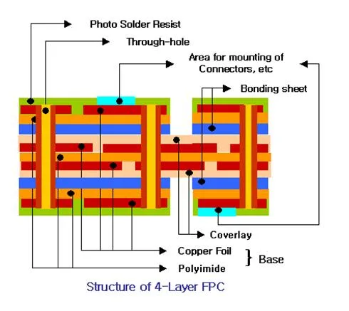
5. Flexible and Rigid-Flex PCBs
Flexible and rigid-flex PCBs utilize flexible materials such as polyimide or polyester as the substrate. These substrates offer excellent mechanical flexibility, allowing them to bend, twist, and conform to irregular shapes. Flexible and rigid-flex PCBs are ideal for applications where space constraints or mechanical flexibility are critical, such as wearable devices, medical implants, automotive sensors, and foldable electronic devices.
6. Composite Substrates
Composite substrates combine multiple materials to achieve specific performance requirements. For example, combining ceramic and metal layers can provide both high thermal conductivity and mechanical strength. Composite substrates are used in a wide range of applications, including aerospace systems, power electronics, RF amplifiers, and high-speed digital circuits.
7. High-Frequency Materials
High-frequency materials are engineered to provide excellent electrical performance at GHz frequencies. These substrates offer low dielectric loss, low dispersion, and stable electrical properties over a wide range of frequencies, making them ideal for high-speed digital, RF, and microwave applications. Common high-frequency materials include PTFE (Teflon), Rogers, and DuPont’s FR-4.
8. Copper Based PCB
Copper-based PCB is a high-end type of metal core PCB, known for its superior thermal conductivity compared to aluminum and iron-based PCBs. It’s particularly suitable for high-frequency circuit designs, environments with significant temperature fluctuations, sophisticated communication equipment, and architectural decoration.
These PCBs come in various finishes, including immersion gold, silver plating, HASL (Hot Air Solder Leveling), and anti-oxidation. They typically feature thicker copper foils (35μm-280μm) to handle high current demands. The thermal conductivity insulating layer, composed of aluminum oxide, silicon powder, and epoxy resin, is crucial to their performance.
Key advantages of copper-based PCBs include low thermal resistance (0.15), good viscoplastic properties, and resistance to thermal aging and stress. The copper substrate, which supports the PCB, plays a vital role in heat dissipation, shielding, and grounding, while also being compatible with standard manufacturing processes like drilling and cutting.
Specialized substrates play a crucial role in the design and performance of PCBs for various applications. By selecting the appropriate substrate material, engineers can optimize the performance, reliability, and functionality of electronic devices across industries.
Choosing the Right PCB for Your Project
Selecting the right PCB for your project is a critical decision that can significantly impact the performance, reliability, and cost-effectiveness of your electronic device. With a wide range of PCB types available, each offering unique features and advantages, it’s essential to consider several factors to ensure you choose the most suitable option for your specific requirements. In this chapter, we will discuss the key factors to consider when selecting a PCB for your project and provide tips for choosing the appropriate PCB type based on different classification criteria.
Factors to Consider
Application Requirements: Understand the specific requirements of your application, including electrical performance, signal integrity, thermal management, and mechanical flexibility.
Budget: Determine your budget constraints and evaluate the cost-effectiveness of different PCB options, considering factors such as material costs, manufacturing processes, and assembly complexity.
Environmental Conditions: Consider the environmental conditions in which the PCB will operate, including temperature extremes, humidity, vibration, and exposure to chemicals or moisture.
Production Volume: Assess the expected production volume of your project, as this will influence the most suitable PCB manufacturing process and volume pricing options.
Lead Time: Evaluate the lead time requirements of your project and choose a PCB manufacturer capable of meeting your timeline without compromising quality.
Regulatory Compliance: Ensure that the selected PCB complies with relevant industry standards, certifications, and regulatory requirements, such as RoHS, REACH, and UL certifications.
Supplier Reputation: Select a reputable PCB manufacturer with a proven track record of quality, reliability, and customer satisfaction. Check reviews, testimonials, and references from previous clients.
Tips for Selecting the Appropriate PCB Type
Classification by Application: Choose a PCB type that aligns with the specific requirements of your application, such as high-frequency RF PCBs for wireless communication devices or flexible PCBs for wearable electronics.
Classification by Production Volume: Select a PCB manufacturing process that matches your production volume, opting for prototype PCBs for small-scale testing and mass production PCBs for large-scale manufacturing.
Classification by Functionality: Consider the functional requirements of your project, such as impedance control for high-speed digital circuits or thermal management for power electronics, and choose a PCB type optimized for those functionalities.
Classification by Specialized Features: If your project requires specialized features or properties, such as high thermal conductivity, mechanical flexibility, or resistance to harsh environmental conditions, opt for PCB types that offer those capabilities, such as metal core PCBs or ceramic PCBs.
Consult with Experts: Seek advice and guidance from PCB design engineers, manufacturers, or industry experts to help you navigate the selection process and make informed decisions based on your project’s specific needs and constraints.
By carefully considering these factors and following these tips, you can choose the right PCB for your project, ensuring optimal performance, reliability, and cost-effectiveness.
Conclusion
In this guide, we have explored the diverse world of Printed Circuit Boards (PCBs), examining various classification methods and types to help you understand the wide range of options available for your projects. From classification by functionality and production volume to specialized substrates and advanced technologies, we’ve covered the essentials of PCB selection.
We began by categorizing PCBs based on functionality, including single-sided, double-sided, multi-layer, rigid, flexible, and rigid-flex PCBs. We then delved into classification by production volume, distinguishing between prototype PCBs for testing and mass production PCBs for large-scale manufacturing. Additionally, we explored specialized substrates such as ceramic, Teflon, and metal core PCBs, as well as advanced technologies like HDI, RF, and microwave PCBs.
Selecting the right PCB for your project can be a complex task, especially given the wide array of options available and the critical role that PCBs play in the overall performance and reliability of electronic devices. If you find yourself unsure or overwhelmed during the selection process, don’t hesitate to reach out for professional advice. PCB design engineers, manufacturers, and industry experts can offer valuable insights and guidance to help you make informed decisions tailored to your project’s specific requirements.
Are you ready to embark on your next PCB project? Whether you’re in need of prototype PCBs for testing, mass production PCBs for large-scale manufacturing, or specialized PCBs with unique features and capabilities, JHYPCB is here to assist you every step of the way. With our expertise, state-of-the-art facilities, and commitment to quality, we strive to deliver superior PCB solutions that meet and exceed your expectations.
Contact JHYPCB today for more information, assistance, or a quote for your PCB project. Let us help you turn your ideas into reality with high-quality, reliable PCBs tailored to your specific needs.
Thank you for choosing JHYPCB as your trusted partner in PCB manufacturing. We look forward to serving you and helping you bring your electronic projects to life!
Frequently Asked Questions (FAQ)
A Printed Circuit Board (PCB) is a flat, rigid or flexible board made of insulating material with conductive pathways etched or printed onto its surface. PCBs serve as the foundation for electronic components and provide a platform for connecting and mounting various electronic devices.
PCBs come in various types, including:
- Single-sided PCBs
- Double-sided PCBs
- Multi-layer PCBs
- Rigid PCBs
- Flexible PCBs
- Rigid-flex PCBs
- High-frequency RF and microwave PCBs
- Metal core PCBs
- Ceramic PCBs
- Teflon (PTFE) PCBs
- HDI (High-Density Interconnect) PCBs
- Prototype PCBs
- Mass production PCBs
Each type has its own unique features, advantages, and applications.
Choosing the right PCB involves considering factors such as:
- Application requirements
- Budget constraints
- Environmental conditions
- Production volume
- Lead time
- Regulatory compliance
- Supplier reputation
It's essential to assess your project's specific needs and constraints and consult with PCB design engineers or manufacturers for expert guidance.
Custom PCBs offer several benefits, including:
- Tailored solutions to meet specific project requirements
- Optimized performance and functionality
- Flexibility and versatility in design
- Enhanced innovation and differentiation
- Improved reliability and cost-effectiveness in the long run
Ensuring the quality of your PCBs involves:
- Choosing a reputable PCB manufacturer with a proven track record of quality and reliability
- Performing thorough testing and inspection throughout the manufacturing process
- Complying with industry standards and regulatory requirements
- Implementing quality assurance measures, such as ISO certifications and continuous improvement processes
The lead time for PCB manufacturing depends on various factors, including the complexity of the design, production volume, and the capabilities of the PCB manufacturer. Typically, lead times can range from a few days for prototype PCBs to several weeks for mass production runs.
To optimize the cost of PCB manufacturing, consider:
- Designing for manufacturability to minimize material waste and assembly complexity
- Consolidating components to reduce assembly time and labor costs
- Choosing cost-effective materials and manufacturing processes without compromising quality
- Negotiating volume pricing discounts with your PCB manufacturer
Common mistakes to avoid in PCB design include:
- Inadequate thermal management
- Poor signal integrity and routing practices
- Incorrect component placement and orientation
- Insufficient clearance and spacing between components and traces
- Lack of consideration for manufacturing constraints and capabilities
Yes, many PCB manufacturers offer technical support and assistance throughout the design, manufacturing, and testing phases of your project. Don't hesitate to reach out to your PCB manufacturer for expert guidance and support.
To contact JHYPCB for more information or a quote for your PCB project, you can:
- Visit our website at www.pcbjhy.com and fill out our online contact form
- Email us at sales@pcbjhy.com
- Call us at +86-0755-23058859
Our team of experts is ready to assist you with your PCB manufacturing needs and provide personalized support tailored to your project requirements.