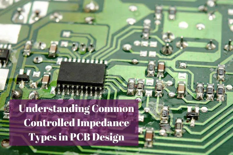
PCBs use copper traces to route signals between components. Controlling the impedance of these traces is essential for proper functioning, especially for high-speed signals. Impedance control means matching the impedance of the PCB traces to the characteristic impedance of the signals they carry.
When the trace impedance is mismatched with the signals, it can cause signal reflection, electromagnetic interference (EMI), and losses. This degrades signal quality and integrity, potentially causing errors, noise, and other issues. Proper control of trace impedance enhances performance and reliability.
In this article, we’ll explain what trace impedance control entails for PCB design. We’ll look at how impedance relates to traces, why it’s crucial to control it, and methods for optimizing trace impedance on your boards. Whether you’re working with digital logic, high-frequency analog, or sensitive applications, understanding trace impedance control is key to success.
What is Impedance?
Impedance refers to the opposition or resistance to the flow of alternating electrical current in a circuit. It applies to AC signals and causes some energy to be lost or reflected back.
Impedance is measured in units called ohms, just like resistance in DC circuits. However, impedance is more complex because it contains both resistive and reactive components.
You can think of impedance like the resistance or friction slowing down the AC signals flowing through a wire or PCB trace. Traces have very low but non-zero impedance. The higher the impedance, the more the signal is impeded.
Impedance also occurs between two adjacent traces, called coupling impedance. This can cause crosstalk and electromagnetic interference. Controlling impedance helps minimize these effects.
On PCBs, we focus on carefully controlling the characteristic impedance of traces to match signal frequencies and prevent reflection. This is key for maintaining signal quality and integrity across the whole path.
Why Control Trace Impedance?
There are a few key reasons proper impedance control is crucial for PCBs:
- Prevents signal reflection – When trace impedance mismatches signal impedance, the signal gets partially reflected back. This distortion causes overshoot, ringing, and loss of signal integrity.
- Reduces EMI – Impedance mismatches between traces increase electromagnetic coupling and interference. Controlled impedance minimizes this.
- Enables high-speed signals – Signals over 100MHz need controlled impedance to prevent reflection and maintain edge rates.
- Maintains signal quality – Controlled impedance keeps signals clean and prevents attenuation, radiated losses, and other issues.
- Allows impedance matching – Trace impedance can be tuned to match driver, receiver, or transmission line impedance for maximum power transfer.
- Limits crosstalk – Coupling between adjacent traces is reduced when their impedances are properly controlled.
In summary, controlled PCB trace impedance is vital for signal clarity, noise reduction, high-speed functionality, and overall reliability. Tight impedance control is essential to handle today’s fast logic, high frequencies, and sensitive applications.
How to Control Trace Impedance?
There are a few key steps involved in optimizing the impedance of traces on a PCB:
- Select stackup materials – The dielectric layers and their thickness strongly influence impedance. Low-Dk materials like FR4 increase impedance.
- Determine trace dimensions – Wider, thicker traces with shorter heights and lower impedance. Trace width can be tuned to hit the target.
- Account for spacing – Tighter spacing between traces lowers impedance due to coupling. Allow enough isolation.
- Use impedance calculators – Online tools like calculators allow rapid iteration to dial-in dimensions.
- Validate with simulations – Model the PCB stackup and traces in 3D EM simulations to verify results.
- Test prototypes – It’s ideal to measure impedance on actual boards and refine if needed.
- Follow layout guidelines – Maintain consistent spacing, routing angles, and reference planes.
By carefully optimizing trace geometry and materials during design, you can achieve the controlled impedance needed for a given application. Prototyping and validation help ensure impedance targets are hit.
When is Impedance Control Used?
Controlled impedance traces are essential for:
- High-speed digital signals – Standards like PCI Express, USB 3.0, SATA III, and HDMI require tight impedance control, often 50 ohms.
- High-frequency analog signals – Radio frequency (RF) boards, oscillators, filters, and wireless chips need tuned trace impedance.
- Clock distribution – Matching trace impedance along clock lines prevents skew between clock nodes.
- Memory interfaces – DRAM and flash memory buses demand proper impedance to limit reflection.
- High-power electronics – IGBTs, motor drives, and power devices need impedance control to reduce switching noise.
- Test and measurement – Impedance matching is vital in oscilloscopes, signal generators, and network analyzers.
In short, any application with fast signals, high frequencies, or low noise requirements relies on precise PCB trace impedance control for success. This includes nearly all modern digital and analog designs.
Conclusion
In summary, controlling the impedance of traces on printed circuit boards is vital for signal integrity. Matching the trace impedance to drivers and transmission lines prevents harmful reflection and EMI.
Carefully designing the PCB stackup, selecting low-loss dielectric materials, and calculating the optimum trace dimensions allow accurately achieving the target impedance. Wider, thicker traces with shorter heights help lower impedance.
Simulation and testing of prototypes validate impedance control and allow refinement before manufacturing. Following impedance-aware layout practices also keeps impedance consistent.
Impedance control enables high-speed digital logic, high-frequency analog signals, noise-sensitive applications, and more. Any design with fast edges or frequencies up to RF ranges relies on proper trace impedance matching.
We hope this article has helped explain the significance of controlled impedance for PCBs. Please reach out if you need assistance designing controlled impedance boards for your next project. Our team of engineers can help advise the best stackup, materials, and layout to achieve your impedance targets.
Related Reading