Introduction
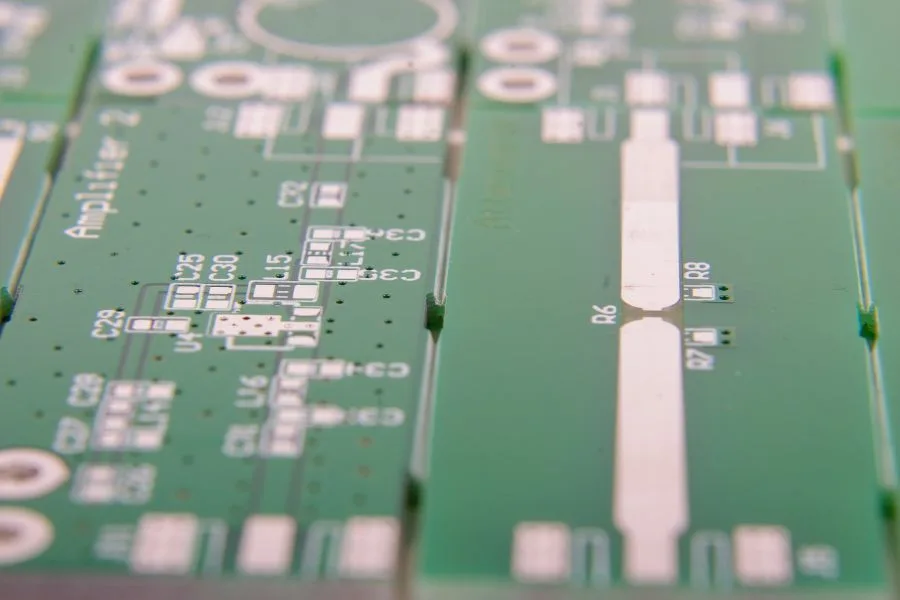
PCBs have become essential components of countless electronic devices we use daily. The manufacturing of each PCB is a complex process involving many steps. One critical stage is PCB profiling, also known as routing, which cuts the individual PCB units out of the larger production panels. Profiling determines the quality of the PCB edges and the accuracy of the final PCB shape. For PCB manufacturers, choosing the optimal profiling technique is crucial for balancing cost, speed, and quality.
As a leading PCB manufacturer based in China, JHYPCB produces high-quality PCBs thanks to our innovative profiling methods. In this article, we will explore the most common PCB profiling techniques used in the industry today – laser cutting, punching, router cutting, and V-cutting. We will compare their working principles, advantages, limitations, and effects on PCB quality. Finally, we will discuss how PCB manufacturers can select the best suited profiling option for their specific production needs and volumes.
Profiling is an indispensable step in transforming production panels to finished PCBs. By understanding the available profiling methods and their characteristics, PCB manufacturers like JHYPCB can optimize this process for greater efficiency, precision, and profitability. Whether you are new to PCB profiling or looking to improve your profiling operations, this article provides useful insights and practical guidance.
Common PCB Profiling Methods
There are several profiling techniques commonly used in PCB manufacturing. Each method has its own sets of advantages and limitations, making it more suitable for certain production scenarios. Choosing the right profiling technique significantly impacts productivity, cost, and PCB quality. PCB profiling methods include laser, punching, router, and V-cut.
Laser Cutting
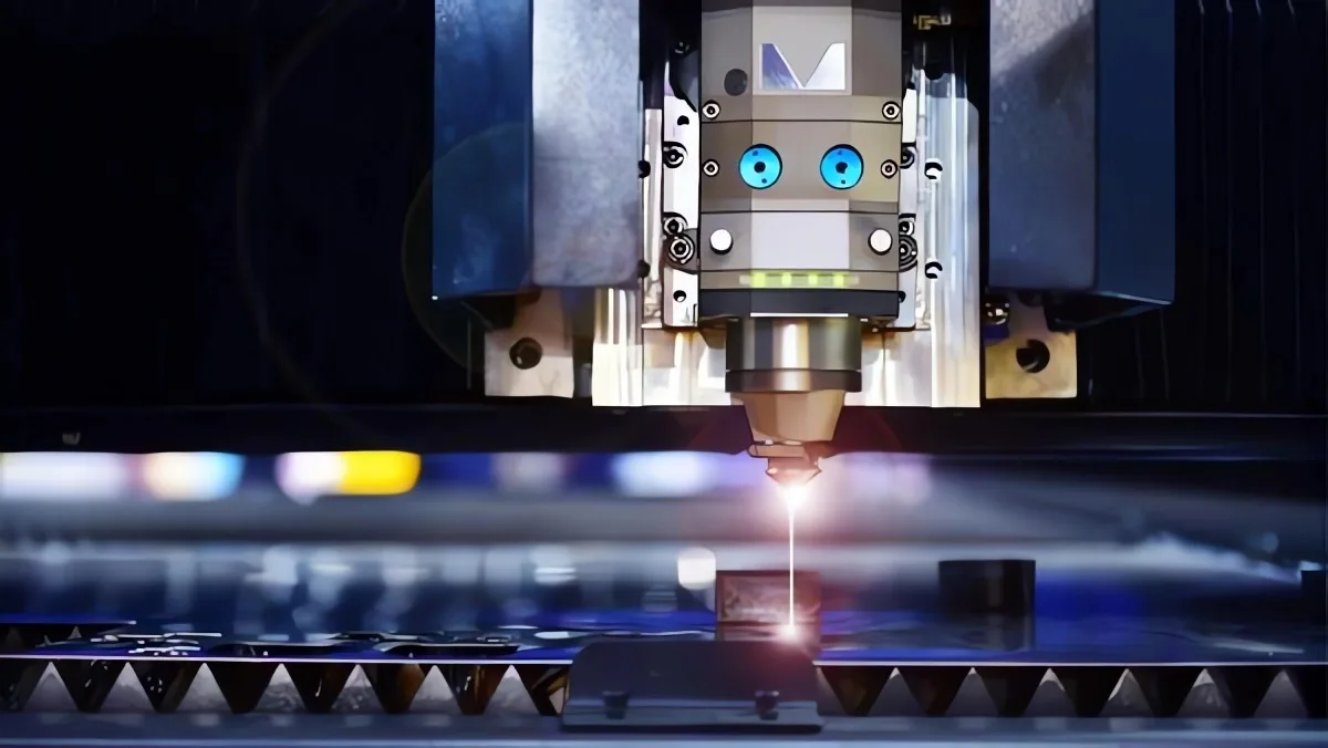
Laser cutting is one of the most precise PCB profiling methods available. It utilizes a high-power laser beam to vaporize material in the path designated for cutting. The laser beam typically has a wavelength of UV or CO2. When focused on the PCB, it provides a narrow cut width and ablates the material cleanly without excessive heat damage.
Compared to mechanical cutting tools, laser offers superior cut quality and precision. The cut edges are clean and smooth without burrs or rough edges. The laser can also cut complex patterns and corners easily. PCB manufacturers can achieve very tight tolerances up to ±0.001 inches with laser profiling.
Since laser cutting is a non-contact process, it eliminates tool wear and deformation issues. The cutting speed can be adjusted easily by controlling laser power and repetition rate. The process generates minimal dust and waste as well.
However, laser profiling requires high initial investment for the laser source, motion system, optics, and operating software. Laser cutting speed is limited compared to mechanical tools. The operational cost is also higher regarding energy consumption and gas usage.
Overall, laser cutting excels in profiling quality and precision. It is best suited for high-end PCBs (Especially for flexible PCBs and rigid-flex PCBs) where edge finish and dimensional accuracy are critical. The non-contact nature enables clean cuts across a wide range of materials too. For low to medium-volume production, laser profiling offers an appealing solution.
Punching
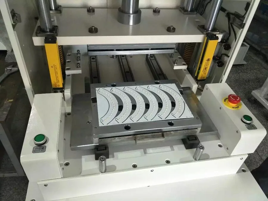
Punching uses a mechanical punching head to cut the profile path on the PCB. The punching head contains a sharp punch that presses down to penetrate the PCB material. As the punch continues to be driven downwards, it severs the material and creates a hole around the PCB profile edge.
Compared to other mechanical cutting methods, punching offers extremely high speeds, capable of profiling over 10,000 holes per minute. It is also very efficient for internal cutouts and void areas. The process can be easily automated linearly.
However, punching does not produce clean-cut edges like a laser. Micro-cracks may form around the hole perimeter, affecting structural integrity. Debris is generated during punching and requires additional cleaning steps.
The punching accuracy is also lower (+/- 0.002 inches) due to potential tool wear and deformation over time. Special hard tools made of carbide or diamond are required to extend tool life.
Overall, punching profiling is ideal when speed and throughput are critical. It works well for high-volume PCB production thanks to automation capabilities. While edge finish is sacrificed, the cost benefits often outweigh this drawback for many PCB manufacturers.
Router Cutting
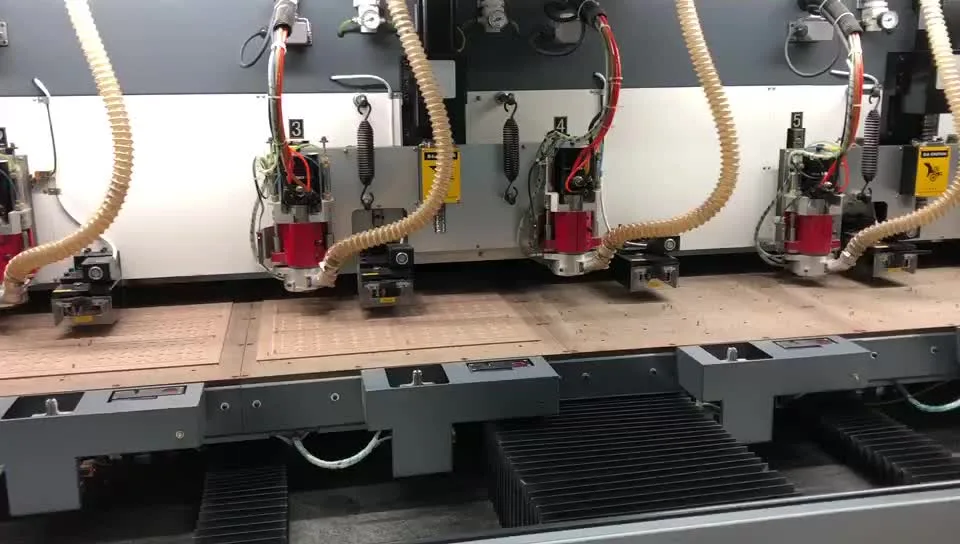
Router cutting uses a rotating cutting tool with a carbide tip to profile the PCB edges. The high-speed spindle spins the router bit at up to 40,000 rpm for removing material efficiently. The PCB is secured to a movable table that shifts along the programmed tool path.
Router profiling can produce good cut quality with smooth edges. The router bit is rigid and accurate, with tight tolerances between ±0.003-0.005 inches. Routers are highly versatile and can make straight and beveled cuts.
Setup time for router cutting is fast, making it efficient for small to medium batch sizes. Automated tool changing enables profiling of complex or internal cutouts as well. Routers have high uptime and are relatively affordable machines.
However, routers produce more debris and noise than laser and punching methods. Tool bits require frequent sharpening or replacement when worn. Routers are also limited in terms of cut radius and contour complexity.
In summary, routing offers a balance of cut quality, flexibility, and cost-effectiveness ideal for many PCB profiling applications. It handles a wide variety of materials well. Routers are productive tools that scale effectively from prototyping to volume production.
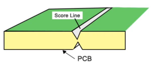
V-Cut
V-cut is the simplest mechanical profiling method for PCBs. It uses a V-shaped cutting tool tipped to a 45-degree angle. The V-Cut blade’s sharp tip penetrates the PCB’s top and bottom sides simultaneously to meet in the middle.
The main advantage of V-Cut is its low cost and speed compared to other methods. Minimal setup is required, and cutting can be performed rapidly. This makes V-Cut suitable for high-volume PCB batch production.
However, the cut quality from V-Cut is relatively poor. The edges are jagged and uneven with potential burrs. The kerf width is also larger, wasting more material. Copper smearing can be an issue without proper blade clearances.
While advances in V-Cut technology like multi-tooth blades have improved quality, it remains a lower precision process. Typical tolerances range from ±0.004-0.008 inches. The cuts are also limited to straight lines and simple geometry.
In summary, V-Cut provides an affordable profiling option ideal for simple board shapes where edge finish is less important. The fast process speeds benefit high-volume PCB production. But cut quality is sacrificed compared to routing, punching, and laser techniques.

How to Choose the Right PCB Profiling Method
Understanding the four major PCB profiling methods, we can now explore the key factors to consider when selecting the optimal technique. The right profiling solution depends on the product requirements, production environment and business priorities.
Firstly, determine the required precision and edge finish quality. High-end boards demand the cleanest cuts and tightest tolerances that laser cutting can provide. For standard quality needs, punching, routing, and V-cut may suffice.
Next, consider the production volume and cycle time targets. Punching and V-cut offer the fastest process speeds for high-volume manufacturing. Lower volume batches are better suited to routing or laser profiling.
The material and board thickness also affect selection. Thicker or advanced materials like RO4350B require more powerful mechanical tools. Lasers can cut thicker boards more easily.
Additionally, evaluate the capital budget, operating costs, and break-even timeframe. Laser has the highest initial cost while V-cut is most affordable. But laser’s lower consumable costs can offset initial investment over time.
Finally, factor in any specialized board shape and cut requirements. Routing has the most profile cut flexibility while V-cut handles only basic geometries.
By weighing all these criteria—quality, speed, materials, costs and capabilities—PCB manufacturers can determine the ideal profiling technology for their situation. Partnering with an experienced supplier can help navigate this key decision as well.
Improving Cut Quality and Productivity
Once a PCB profiling method is selected, manufacturers can take steps to optimize the process for greater cut quality and productivity.
For mechanical profiling tools like routers and punches, regular maintenance and sharpening is essential. Replacing worn bits and maintaining proper blade clearances improves edge finish and precision. Streamlining tool changeovers also reduces downtime.
Adjusting feed rates, spindle speeds, and depth of cut will enhance performance based on the material properties. Proper fixturing of the PCB panels is also crucial for accuracy.
With laser cutting, parameters like power, pulse rate, and focal point position can be tuned to maximize cut quality and speed for the material thickness. Gas type and pressure also impact performance.
Software improvements can boost profiling efficiency. Optimizing the cut path sequence and travel motions minimizes rapid movements and lowers cycle times. Nesting multiple PCBs on the panels also improves material utilization.
Finally, inspecting cut quality and implementing feedback loops allows continuous enhancement. Data collection to identify potential process drifts enables preventive action.
By adopting these optimization practices, PCB manufacturers can achieve better profiling results, reduced costs, and higher customer satisfaction. The pursuit of excellence in PCB profiling requires integration of technology, process, and people.
Conclusion
In conclusion, PCB profiling is a critical manufacturing process that impacts cost, quality, and efficiency. We have explored four prevalent profiling methods—laser cutting, punching, routing, and V-cut—and their relative strengths and weaknesses.
Key factors to consider when selecting a profiling technique include precision requirements, production volume, material properties, operating costs, and design complexity. Optimizing the chosen profiling method through machine maintenance, parameter adjustment, and software improvements can further enhance performance.
By understanding the principles behind each profiling option and implementing best practices, PCB manufacturers can achieve improved cut quality, higher yields, and better productivity. As volumes increase and designs become more advanced, choosing the right profiling technology becomes even more crucial.
JHYPCB, as an expert PCB manufacturing partner, stays abreast of the latest developments in profiling and other PCB fabrication processes. By leveraging our experience and technical capabilities, we deliver exceptional quality and value to customers across industries.
We hope this article provides useful guidance to PCB producers evaluating their profiling operations. Please reach out for any questions on implementing an optimized, cost-effective profiling solution for your production needs.
Related Reading