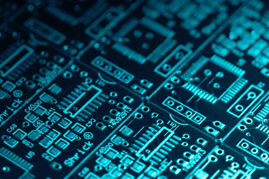
Multilayer PCBs, also known as multilayer printed circuit boards, are essential components of electronic devices used in everything from smartphones and computers to automobiles and medical equipment. Unlike single-layer PCBs, multilayer PCBs consist of multiple conductive materials separated by insulating layers, allowing for a more compact and efficient design.
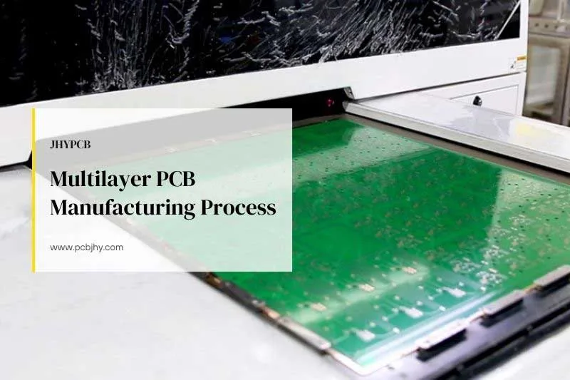
The manufacturing process of multilayer PCBs is complex and involves several stages, including design, pre-production, inner and outer layers production, and final production. Each stage requires precision and expertise to ensure the final product meets the specifications.
In this guide, we will provide an overview of the multilayer PCB manufacturing process, from design to final production, and highlight the importance of this technology in modern electronic devices.
Defining Multilayer PCBs
Multilayer PCBs are printed circuit boards with more than two layers of conductive material separated by insulating layers. These layers are interconnected through plated through holes, vias, or buried vias, allowing for the transfer of electrical signals between layers.
The number of layers in a multilayer PCB can vary, ranging from four to dozens of layers, depending on the complexity of the circuit design and the required performance specifications. Multilayer PCBs, such as smartphones, computers, and medical equipment, are widely used in electronic devices that require a high degree of functionality and compactness.
Importance of Multilayer PCBs
The importance of multilayer PCBs lies in their ability to provide a compact and efficient solution for complex circuit designs. With the increasing demand for smaller and more powerful electronic devices, multilayer PCBs have become essential to meet these requirements.
Multilayer PCBs offer several advantages over single-layer PCBs, such as reduced noise interference, better signal integrity, and improved thermal management. These benefits make multilayer PCBs ideal for high-speed data transmission, high-frequency signals, and power management applications.
In the next sections, we will provide a detailed overview of the multilayer PCB manufacturing process, highlighting the key steps involved in producing a high-quality multilayer PCB.

Multilayer PCB Manufacturing Process
Step 1: Design and Layout
The design and layout stage is the first and most crucial step in the multilayer PCB manufacturing process. The goal of this stage is to create a design that meets the functional and performance requirements of the electronic device while also considering the physical limitations of the PCB.
- PCB Design Software:
PCB design software, such as Altium, Eagle PCB, and KiCAD, is used to create the layout of the PCB. The software allows the designer to create a schematic diagram of the circuit and then convert it into a physical layout that can be manufactured.
- Stackup Design:
The stackup design is the process of determining the number of layers and the thickness of each layer in the PCB. The designer must consider factors such as the number of components, signal integrity, power distribution, and thermal management when deciding on the stackup design.
- Routing and Traces:
The routing and traces refer to connecting the various components on the PCB. The designer must ensure the routing and traces are optimized for the desired performance, such as signal integrity and power distribution. In addition, the designer must follow the design rules for the PCB to ensure manufacturability.
- Signal Integrity Analysis:
Signal integrity analysis is a crucial step in the design and layout stage, as it helps to ensure that the signals on the PCB are transmitted correctly and without interference. This analysis involves simulating the performance of the PCB using specialized software to identify and eliminate any potential signal integrity issues.
Once the design and layout of the multilayer PCB is complete, the next step is pre-production. The materials and processes necessary for manufacturing the PCB are selected and prepared in the pre-production stage. This stage is essential to ensure that the final product meets the required specifications and standards.

Step 2: Pre-production
The pre-production stage is a critical step in the multilayer PCB manufacturing process. This stage involves selecting the materials and processes necessary for manufacturing the PCB and preparing them for production. The pre-production stage is essential to ensure that the final product meets the required specifications and standards.
The selection of materials for the multilayer PCB is crucial to ensure the performance and reliability of the final product. The materials used for the PCB include copper foil, prepreg, and core materials.
Copper foil is used to create the conductive layers of the PCB. The thickness of the copper foil depends on the required current-carrying capacity and the impedance of the circuit.
Prepreg is an insulating layer between the copper layers, and core materials provide the mechanical support for the PCB.
The selection of materials is based on the performance requirements of the final product and the available manufacturing processes.
Learn More:
- Complete Guide for PCB Material
- Materials Used for High Tg PCBs: A Comparison and Selection Guide
- What are the Materials for Flex Circuits?
- Process Selection:
The selection of the manufacturing process for the multilayer PCB is also critical to ensure the quality and reliability of the final product. The manufacturing process involves several steps, including drilling, plating, lamination, and etching.
The manufacturing process selection depends on the complexity of the PCB design, the number of layers, and the required specifications.
- Panelization:
Panelization involves arranging the individual PCBs on a larger panel to optimize the use of manufacturing equipment and reduce material waste. Panelization also helps to ensure that the PCBs are separated correctly after manufacturing.
- Drilling and Plating of Through-holes:
Drilling and plating of through-holes are critical steps in the manufacturing process of multilayer PCBs. Through-holes provide the connection between the layers of the PCB. The drilling process involves drilling holes through the core and prepreg layers, and the plating process involves depositing copper on the walls of the holes to create a conductive path.
- Lamination of Core Layers:
To create a solid panel, the lamination process involves bonding the core and prepreg layers together under heat and pressure. The number of layers and the thickness of the prepreg used in the lamination process depend on the design of the multilayer PCB.
- CAM Data Preparation:
Computer-aided manufacturing (CAM) data preparation converts the PCB design and layout into a format that the manufacturing equipment can use. This process involves converting the design data into machine-readable instructions controlling manufacturing equipment.
The CAM data preparation includes data verification, tooling, and fixture design. This process ensures that the manufacturing equipment can produce the PCB accurately and efficiently.
Once the pre-production stage is complete, the next stage is the production stage. In the production stage, the materials and processes selected in the pre-production stage are used to manufacture the multilayer PCB.
Step 3: Inner Layers Production
The inner layer production is a crucial stage in the manufacturing process of multilayer PCBs. The inner layers are sandwiched between the outer layers and typically comprise copper foil and prepreg.
- Inner Layer Imaging:
The first step in the inner layer production process is inner layer imaging. This process involves transferring the circuit pattern from the design data onto the copper layer of the inner layers. The imaging process uses a photoresist material applied to the copper layer.
The photoresist is exposed to light through a film or mask that contains the circuit pattern. The areas exposed to light become hardened, while the unexposed areas remain soft. The soft areas are then washed away, leaving behind the circuit pattern on the copper layer.
- Etching:
After the imaging process, the next step is etching. Etching is the process of removing the unwanted copper from the inner layers to create the circuit pattern. The etching process involves immersing the inner layers in an etching solution that dissolves the exposed copper.
The etching solution is typically a mixture of acids, such as ferric chloride or ammonium persulfate. The etching solution only dissolves the exposed copper, leaving the unexposed areas untouched. The etching process is closely monitored to ensure the circuit pattern is precisely formed.
- Stripping and Cleaning:
After the etching process, the next step is stripping and cleaning. Stripping is the process of removing the remaining photoresist material from the inner layers. The stripping process uses a solution that dissolves the photoresist material but does not affect the copper layer.
After stripping, the inner layers are cleaned to remove any remaining residues and contaminants. The cleaning process is critical to ensure the adhesion of the prepreg and the outer layers.
- Lamination:
The final step in the inner layer production process is lamination. The inner layers are sandwiched between prepreg layers and bonded under heat and pressure to form a solid panel. The lamination process involves the same steps as the core layer lamination, including stacking, alignment, and bonding.
The number and thickness of the prepreg layers used in the lamination process depend on the design of the multilayer PCB. The lamination process is critical to ensure that the inner layers are securely bonded and that the panel is flat and uniform in thickness.
Once the inner layer production is complete, the next step is the outer layer production. In the outer layer production process, the outer layers are produced, and the inner layers and outer layers are bonded together to form a complete multilayer PCB.
Step 4: Outer Layers Production
The outer layer production process involves manufacturing the top and bottom copper layers of a multilayer PCB. The outer layers are bonded to the inner layers to create the multilayer PCB.
- Outer Layer Imaging:
The first step in the outer layer production process is outer layer imaging. This process is similar to the inner layer imaging process and involves transferring the circuit pattern from the design data onto the copper layer of the outer layers. The imaging process uses a photoresist material applied to the copper layer.
The photoresist is exposed to light through a film or mask that contains the circuit pattern. The areas exposed to light become hardened, while the unexposed areas remain soft. The soft areas are then washed away, leaving behind the circuit pattern on the copper layer.
- Etching:
After the imaging process, the next step is etching. Etching is the process of removing the unwanted copper from the outer layers to create the circuit pattern. The etching process involves immersing the outer layers in an etching solution that dissolves the exposed copper.
The etching solution is typically a mixture of acids, such as ferric chloride or ammonium persulfate. The etching solution only dissolves the exposed copper, leaving the unexposed areas untouched. The etching process is closely monitored to ensure the circuit pattern is precisely formed.
- Stripping and Cleaning:
After the etching process, the next step is stripping and cleaning. Stripping is the process of removing the remaining photoresist material from the outer layers. The stripping process uses a solution that dissolves the photoresist material but does not affect the copper layer.
After stripping, the outer layers are cleaned to remove any remaining residues and contaminants. The cleaning process is critical to ensure the adhesion of the outer and inner layers.
The next step in the outer layer production process is solder mask application. Soldermask is a protective coating applied over copper traces to protect them from oxidation and to prevent unwanted solder bridges during assembly.
The solder mask is typically a liquid epoxy ink applied using screen printing. The solder mask is cured under UV light to harden it and provide a durable coating resistant to solvents and abrasion.
The final step in the outer layer production process is surface finish application. Surface finish is a coating applied to the copper pads to protect them from oxidation and to ensure good solderability during assembly.
There are several types of surface finishes available, including HASL (Hot Air Solder Leveling), ENIG (Electroless Nickel Immersion Gold), and OSP (Organic Solderability Preservatives). The type of surface finish used depends on the application and the design requirements of the multilayer PCB.
Once the outer layer production process is complete, the next step is to bond the outer layers to the inner layers using the lamination process. The lamination process involves using heat and pressure to bond the layers and form a multilayer PCB.
Step 5: Final Production
- CNC Routing:
CNC routing uses a computer-controlled machine to cut the multilayer PCB into its final shape. The machine uses a drill bit to cut the board along the outline specified in the design files. CNC routing can also cut slots and holes in the PCB.
- V-Scoring and Depanelization:
V-scoring and depanelization are processes used to separate the individual PCBs from the panel. V-scoring involves cutting grooves on the top and bottom of the panel, which allows the individual PCBs to be easily broken apart. Depanelization is the process of separating the PCBs from the panel.
- Electrical Testing:
Electrical testing ensures that the multilayer PCB meets the required specifications. This involves testing for continuity, shorts, and opens. Automated testing equipment is often used to perform these tests, which can be done quickly and accurately.
- Quality Control:
Quality control is the process of ensuring that the multilayer PCB meets the required quality standards. This involves inspecting the PCB for defects and ensuring it meets the design files’ specifications. Quality control can be performed manually or using automated inspection equipment.
Conclusion
In summary, multilayer PCB manufacturing involves several complex processes, including design and layout, pre-production, inner layers production, outer layers production, and final production. Each stage requires careful attention to detail and quality control measures to ensure the final product meets the required specifications.
Multilayer PCBs are essential components in modern electronic devices, and their quality is critical to the device’s overall performance. Poor-quality multilayer PCBs can lead to circuit failures, malfunctioning devices, and potentially dangerous situations. Therefore, it is essential to work with a reputable and experienced multilayer PCB manufacturer who prioritizes quality control at every stage of the production process.
By partnering with a high-quality multilayer PCB manufacturer, you can rest assured that your PCBs will meet the required specifications and provide reliable performance. With advances in technology and manufacturing techniques, multilayer PCBs are becoming more efficient, durable, and capable of meeting the demands of increasingly complex electronic devices. As such, investing in high-quality multilayer PCBs can help ensure the success and longevity of your electronic devices.
JHYPCB: Your Trusted Multilayer PCB Manufacturer
If you’re looking for a trustworthy and experienced multilayer PCB manufacturer, look no further than JHYPCB. Our commitment to quality and customer satisfaction is second to none. We use the latest technology and manufacturing techniques to produce high-quality multilayer PCBs that meet the demands of even the most complex electronic devices.
Contact us today to learn more about our services and how we can help you bring your electronic device to life. With our expertise and attention to detail, you can trust that your multilayer PCBs will be of the highest quality and provide reliable performance. Let us help you take your project to the next level.
Related Reading