- Base Material Preparation
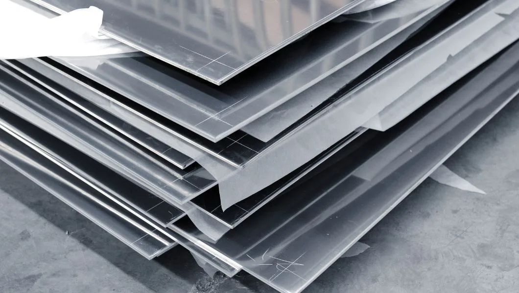
The first step in manufacturing a metal core PCB is preparing the base metal material. The base forms the foundation on which the entire board is built. The type of metal selected depends on the thermal and mechanical requirements of the application. Popular options include:
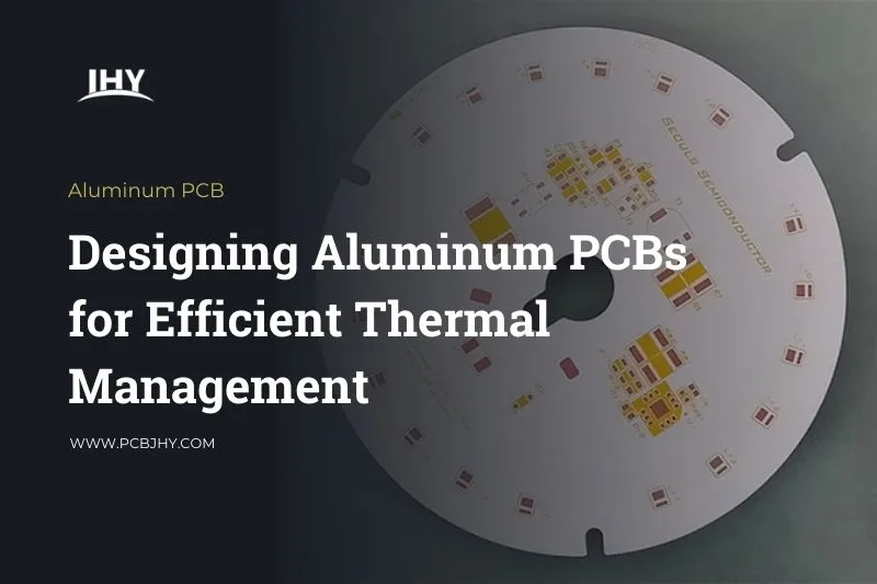
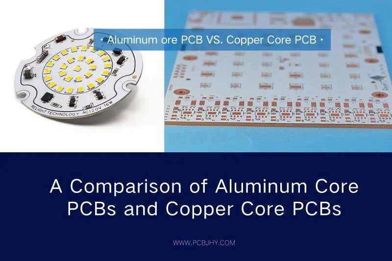
- Aluminum: Offers superior thermal performance due to its excellent thermal conductivity. It is also lightweight and cost-effective. However, aluminum can be prone to oxidation and has lower rigidity than copper.
- Copper: Provides very high thermal conductivity coupled with excellent mechanical strength. Copper offers better solderability than aluminum. However, copper is heavier and more expensive.
The base metal must have a high-quality finish and smooth surface for the subsequent laminating processes. Common surface treatments include chemical etching, mechanical polishing, and oxide coating. The base metal sheets are precision cleaned to remove any contaminants like oils, oxides, and dust particles.
Next, the sheets are cut to the required PCB panel sizes taking into consideration the final board dimensions and any margin areas. Precise machining is critical to minimize wastage and ensure panel flatness.
The treated metal base forms the foundation of the PCB sandwich. The next steps focus on building up the circuit layers on this core.
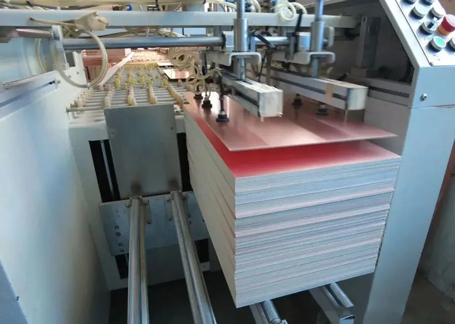
PCB Copper Clad Laminate Cutting
- Imaging/Lamination
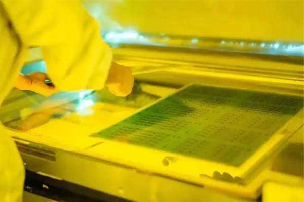
With the metal base ready, the next phase is to create the conductive circuitry on top of it through a series of imaging and lamination processes.
First, a layer of photoresist is applied on the cleaned metal surface. The photoresist coating is evenly spread using a specialized laminating machine.
Next, the actual circuit layout artwork is transferred onto the photoresist layer. This is done by exposing the board to UV light through the artwork pattern. The exposed areas undergo a chemical reaction that allows its removal in the subsequent developing process.
The dielectric layer, typically made of a material like polyimide, is now laminated on top of the imaged photoresist. This electrically insulates the metal base from the circuits. Lamination is done under high heat and pressure to create a strong bond.
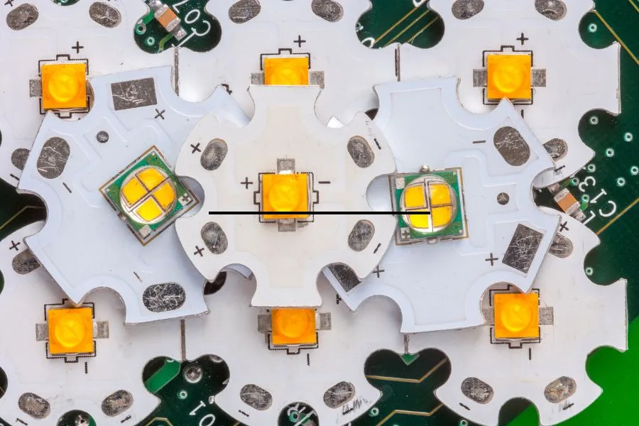
Finally, a sheet of copper foil is layered on top, which will form the actual circuit traces after etching. The stacked “sandwich” is again heated and pressed to fuse the layers together into a composite PCB panel ready for etching.
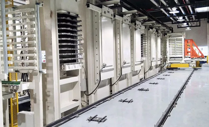
PCB Lamination
- Etching
The core role of etching is to remove unwanted copper so that only the intended circuit paths remain. This is done by taking advantage of the photoresist patterning completed in the previous imaging steps.
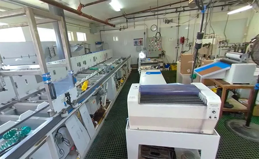
The PCB panel is first immersed in an etchant solution, typically ferric chloride or ammonium persulfate. The solution chemically dissolves away the exposed copper that is unprotected by the photoresist. This reveals the circuit patterns transferred from the original artwork.
Spray etching is an efficient alternative to dip etching. High-pressure etchant jets impinge on the panel surface to rapidly dissolve copper. Spray etching also allows for improved process control.
After etching, the photoresist layer must be stripped away. This reveals the pristine copper traces sealed by the solder mask. An anti-tarnishing treatment is applied to prevent the etched copper traces from oxidizing.
Etching is a critical step that transforms the blank copper layer into the intricate printed circuit artwork. The accuracy of etching determines the quality of circuits. A precisely controlled etching process is crucial for meeting fine line width and spacing requirements.
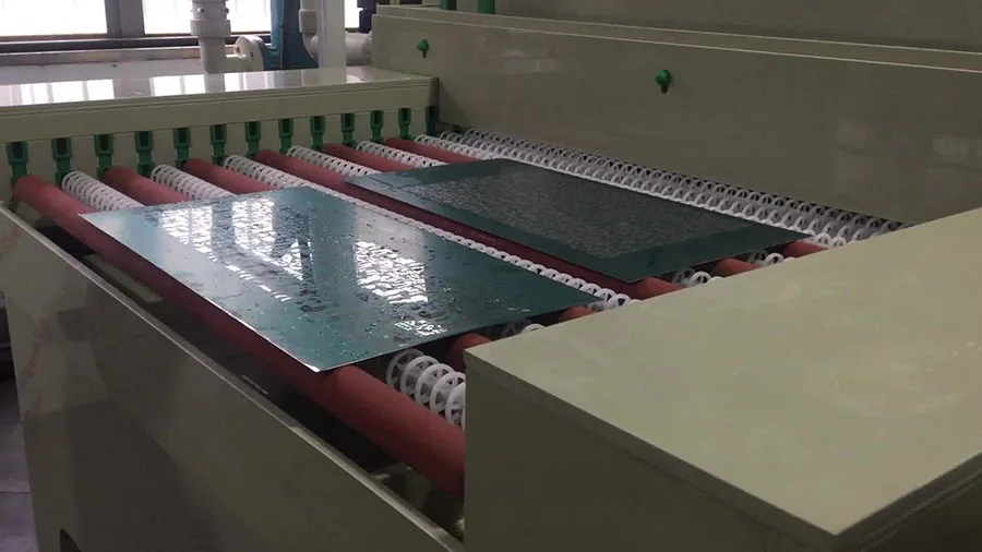
PCB Etching
- Hole Drilling
Now that the circuit layers are formed, the next step is to drill holes that allow component connections across layers.
Holes are required for mounting components to the board and for creating interlayer connections called vias. High-speed drilling machines are used to accurately drill thousands of holes in each panel.
Common drilling techniques include mechanical drilling, laser drilling, and plasma drilling. Mechanical drilling using carbide bits is suitable for most typical PCBs. Laser drilling provides excellent precision for drilling microvias under 0.005 inches.
Drilled holes must make a strong connection between layers. This requires metalizing the hole walls. Electroless copper plating is commonly used to deposit a thin copper layer onto the hole walls and interconnect the layers.
In designs with multiple layers, blind and buried vias electrically connect inner layers without spanning the entire PCB thickness. Constructing such complex via structures requires precision drilling and careful hole metallization.
The drilling and plating processes transform a simple layered board into an intricate 3D circuit structure ready for component mounting and soldering.
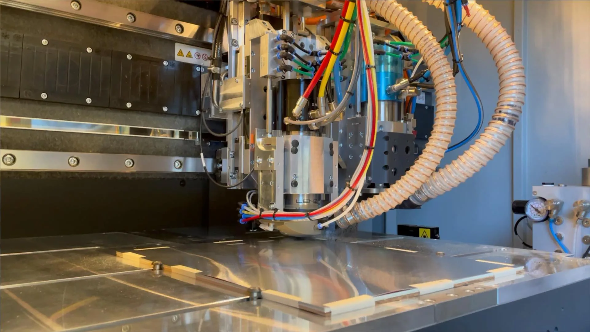
PCB Drilling
- Solder Mask Application
Solder masks are coatings applied to protect copper traces from oxidation and prevent solder bridges between adjacent pads.
The solder mask is typically an epoxy-based polymer that is applied in liquid form as a thin coating. It is spread evenly over the entire PCB surface using curtain coating or spray methods.
The coating is then partially cured using UV light or heat. Next, the coating is selectively exposed through artwork patterns. This transfers the solder mask openings onto the coating.
The board is then developed, washing away the exposed solder mask areas. This leaves solder pads and traces exposed while the rest of the copper surface remains protected.
Finally, the solder mask is fully cured to achieve optimal mechanical and chemical resistance. Curing is done using hot air ovens to create cross-linking between the epoxy polymer chains.
The solder mask color can be varied based on application needs. Common options are green, red, blue, and black. Automated optical inspection verifies the quality of the solder mask application.
This completes the PCBA structure. The board next moves to the finishing stages.
Solder mask applications
- Surface Finishing
Surface finishing processes are applied to protect exposed copper and facilitate soldering. These finishing treatments complete the PCB fabrication.
Exposed copper is susceptible to oxidation and discoloration. So the first step is to coat the exposed copper with an organic solderability preservative (OSP). OSP contains azole compounds that adhere to the copper surface preventing oxidation.
Nickel/gold (Ni/Au) plating can also be applied to provide excellent solderability while avoiding oxidation. The nickel layer acts as a barrier while the gold outer layer provides superior conductivity and corrosion resistance.
For specialized applications, Immersion Silver or Immersion Tin finishes are plated to enhance solderability. The choice of finish depends on soldering requirements and budget considerations.
Next, markings are printed identifying components positions, test points, board name, logo, etc. This legend printing helps guide SMT assembly and assists in troubleshooting. Inkjet printing offers a flexible and efficient marking process.
This concludes the PCB fabrication process. The board now undergoes electrical and quality testing before shipment to the customer. The surface finishing provides the final touches creating a solderable and enduring PCB product.
PCB surface finish process
- Electrical Testing
Before the fabricated PCBs are shipped to customers, they must pass a battery of electrical tests. Testing ensures the boards function correctly and meet design specifications.
The first test is an open/short circuit check. This verifies all intended connections exist without any shorts between unrelated copper traces. Testing probes check for resistance across circuits.
An automated optical inspection looks for any physical defects like scratches, nicks, missing pieces, etc. Any boards with visible defects are marked for rejection.
Impedance testing validates the dielectric and trace dimensions to match the intended impedance values. This is important for high-frequency signals in circuits.
For multilayer boards, a bed-of-nails test probes each circuit node by making contact through test points and vias. Capture probes to detect any erroneous connections.
Boards also undergo functional testing according to the customer’s product requirements. Selected devices simulate actual integrated circuits.
The testing data is recorded and analyzed to identify any process improvements needed. Statistically low defect rates ensure reliable and consistent product quality.
Passing all the qualification tests completes the fabrication process, making the boards ready for volume production and delivery.
Flying probe test
- Final Processing
Once fabricated PCBs pass all electrical tests, they undergo final processing steps to complete the boards ready for shipment.
The PCB panels are sliced into individual boards based on the customer’s specifications using either routing, scoring, or v-cutting. Any special punched holes or cutouts are also completed.
Edge beads are usually added along the perimeter of each board. This helps protect the edges from chipping and moisture ingress. Bevelling routs chamfers along board edges for an enhanced appearance.
Conformal coatings can be applied to provide environmental protection for boards that will operate in demanding conditions like high humidity or vibration. Coatings are applied via spraying or selective dipping.
Solder paste is screen printed on boards that will directly undergo component placement and reflow soldering at the customer’s facility. This provides solder ready boards.
Each board now undergoes a final quality inspection looking for defects like nicks, scratches, or coating imperfections. Approved boards are packed and shipped using anti-static bags and proper cushioning materials.
This concludes transforming raw materials into complete PCBs ready for end use. Proper final processing ensures the boards reach customers in optimal condition.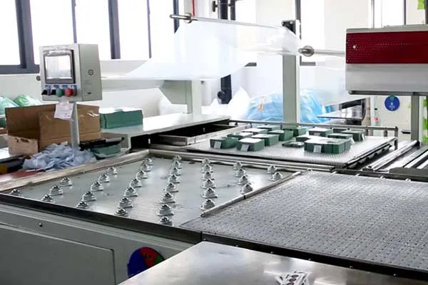
Packing and delivery