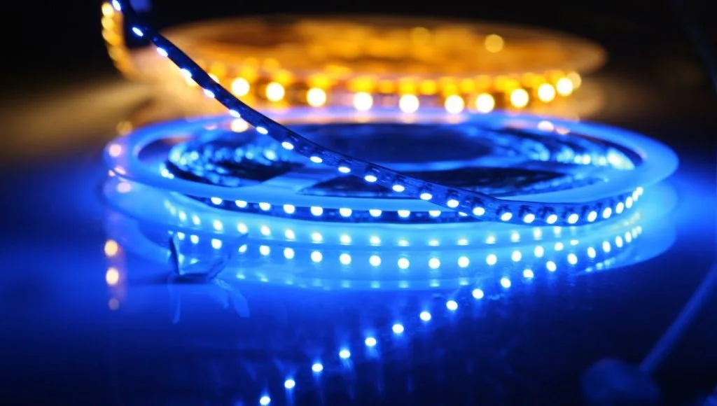
LED lighting is becoming increasingly popular in applications ranging from consumer electronics to automotive lighting. As demand grows, manufacturers need to optimize their PCB design and assembly processes to achieve the high quality and performance that LEDs require.
This LED PCB design guide provides key considerations, tips, and best practices for electronics manufacturers. Optimizing the design and layout is crucial for ensuring the proper functioning, longevity, and brightness of LED circuits. Factors like thermal management, current capacity, and manufacturability must be addressed early when developing a new LED PCB.
The layout and trace routing on the PCB establish the foundation for delivering uniform current to LEDs. Thoughtful component placement and spacing will enhance thermal dissipation across the board. Design choices like layer stackup and via design also impact thermal and current management. Additionally, the PCB fabrication and assembly process must produce highly reliable solder joints, components bonding, and quality control.
By following the recommendations in this guide, manufacturers can develop LED PCB designs that meet performance and lifespan requirements. A well-designed board will provide even illumination, reduce power loss, and prevent overheating. Working closely with your PCB production partners ensures the design is optimized for manufacturability. The end result is a reliable, cost-effective PCB assembly that leverages the latest LED technology.
The subsequent sections will delve into key considerations around layout, thermal design, high-current handling, manufacturing processes, and testing procedures. Following best practice guidelines at every stage of the design process enables creating durable and high-performing LED boards.
PCB Layout Guidelines
The layout and routing of the PCB serves as the foundation for an effective LED board design. The following layout best practices will optimize light distribution, thermal dissipation, and current delivery.
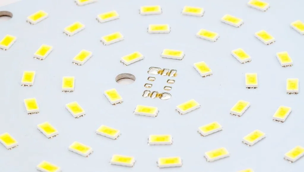
Component placement is a critical first step. LEDs should be arranged to achieve uniform light output in the desired illumination pattern. Placing LEDs in linear rows or symmetrical grids often provides the best results. Ensure adequate spacing between LEDs and other components to prevent crowding or shadowing effects.
Trace width must be calculated based on the expected current draw of each LED. Wider traces help safely accommodate the high current levels. Use online trace width calculators to determine appropriate widths based on current, PCB material, and temperature rise. Minimizing trace lengths also helps reduce unwanted voltage drops across the board.
Adequate spacing should separate traces from planes or pads carrying high current. Allow at least 3x the trace width for proper isolation and heat dissipation. Traces should avoid running directly underneath hot components like LEDs or driving chips.
For optimal thermal performance, a 4-layer board is recommended. This allows a full ground plane and power plane to distribute current and heat evenly. Additional inner layers can be added for complex or high-power boards as needed. thermal relief cutouts and anti-pads around pads and vias facilitate heat dissipation.
Following these PCB layout guidelines will help avoid common problems like luminous flux drops, uneven lighting, and overheating. Proper planning and layout set the stage for a LED board that delivers superior illumination, efficiency, and longevity.

Thermal Management Strategies
Managing heat buildup is imperative for LED reliability and brightness. LEDs generate significant heat during operation which must be dissipated properly. Effective thermal management should be incorporated throughout the PCB design process.
Several techniques can enhance heat spreading and dissipation across the board:
- Use large thermal pads connected to internal copper planes to draw heat away from hot components. The LED mounting pads should be as large as possible.
- Incorporate thermal vias underneath devices and in heat zones to conduct heat to inner or bottom layers. These act as “chimneys” for vertical heat transfer.
- Add thermal relief cutouts and anti-pads in the copper planes surrounding LED pads and vias. This improves horizontal heat spreading.
- Specify PCB substrate materials such as metal core PCBs or ceramic PCBs to maximize thermal conductivity.
- Use finishes like immersion silver plating that transfer heat efficiently from pads to solder.
- Strategically place test points to monitor temperatures during testing and troubleshooting.
- Sandwich the board between thermally conductive insulation layers or heatsinks.
The proper thermal design prevents LED junction temperatures from exceeding recommended limits. This helps maintain brightness, avoid color shifting, and extend the LED lifespan. Following thermal best practices results in more reliable, uniform, and brighter LED illumination.
Accommodating High Current Levels
LEDs require very high forward current levels to produce bright output. The PCB design must deliver the necessary current through robust traces and minimal voltage drops.
Using thicker copper weights for current-carrying traces enhances the current capacity. Aim for 2oz copper or higher on the outer layers. For extremely high currents, consider copper thicknesses up to 5oz.
Minimize the number of drill holes and vias intersecting high current paths. Each via contributes unwanted resistance and heating. Use larger diameter vias where needed to reduce resistance.
Incorporate large copper power and ground planes to evenly distribute current across the board. This also enhances thermal dissipation. The power plane should be sufficiently wide to handle the required current levels.
Current-sense resistors can monitor power for troubleshooting but add resistance. Minimize their number and footprints. Where needed, specify high power, low resistance shunt resistors.
If possible, specify surface mount LEDs and components to avoid drill holes. Otherwise, use annular ring standards to ensure reliable hole connections.
Test boards under maximum expected current loads and monitor voltage drops. Measure points near the end of a long trace run to identify potential weak points.
Adequately accommodating the LED power demands will result in bright, consistent illumination across all LEDs. Following high-current design principles prevents trace overheating, voltage drops, and other issues caused by excessive resistance.

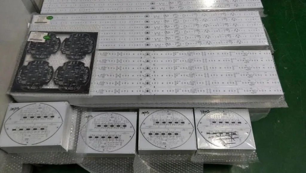
Manufacturing Process and Testing
Robust quality control and testing processes ensure reliable PCB production and assembly. Closely monitoring key parameters verifies the board meets specifications.
For SMT LEDs, use solder paste designed for heat-sensitive components. Nitrogen reflow helps prevent oxidation. Inspect solder joints and fillets thoroughly after reflow. X-ray inspection can check for hidden flaws.
For through-hole LEDs, use redundant solders holes and/or screws for mechanical strength. Flux helps avoid solder bridges between connections. Clean thoroughly after soldering.
100% AOI inspection after SMT assembly catches common defects like missing or misaligned components. ICT testing verifies net connectivity and detects short circuits.
Perform in-circuit testing to validate proper current draws and LED functionality. Programmable power supplies enable current ramping and thermal cycling tests.
Monitor LED voltages and junction temperatures during hot testing at maximum current loads. Use thermal imaging cameras to identify hot spots. Burn-in screening accelerates early component failures.
QC testing should include metrics like luminous flux, chromaticity, LED orientation, and markings. Visually inspect the illumination pattern for uniformity.
Rigorous testing protocols applied through volume production ensure consistently high quality. This allows manufacturers to confidently deliver reliable, high-performing LED boards.
Conclusion/Summary
In summary, designing and manufacturing high-quality LED PCBs requires attention to factors spanning layout, thermal management, current capacity, production processes, and testing.
PCB layout sets the stage for even light distribution and minimal voltage drops. Effective heat sinking and thermal plane design prevent overheating issues. Robust power traces and planes accommodate high currents. Rigorous testing and inspection at multiple stages verify performance and reliability.
Close collaboration between design engineers and manufacturing partners ensures the PCB design is optimized for manufacturability and quality control. With careful planning and adherence to best practices, electronics manufacturers can develop LED boards that deliver superior illumination, efficiency, and lifespans.
As LED technology continues advancing, PCB designs must evolve as well. Emerging trends like chip-scale LED packaging and alternate substrate materials provide new options. However, the fundamentals of good thermal, mechanical, and electrical design remain universal. This LED PCB design guide aimed to provide a strong foundation for approaching LED boards.
By following these guidelines and recommendations, manufacturers can tap the full potential of LEDs. Properly designed PCBs will illuminate products and solutions with reliable, energy-efficient, and visually stunning LED lighting for years to come.
Related Reading:
- The Best Materials for LED PCB Boards
- Expand Your LED Lighting With Custom LED PCBs
- Speed Up Your PCB Design with Double Sided Prototyping
- Multilayer PCB Design Guide: A Comprehensive Overview
- Designing Aluminum PCBs for Efficient Thermal Management
- Rigid Flex PCB Design Guidelines: Key Guidelines to Follow
- High Tg PCB Design Guidelines: Best Practices and Tips for Success
- Design Considerations for Metal Core PCBs: Tips and Tricks for Optimal Performance
- How to Design a Heavy Copper PCB?