When embarking on a new PCB hardware project, one of the first questions designers and engineering teams need to answer is: “What will the bare board fabrication cost?” Understanding key cost drivers enables intelligent design decisions to optimize expenses. It also facilitates budgeting and early scoping of a bill of materials.
This article provides an in-depth look at the major factors that influence bare PCB manufacturing costs. For electronics companies and designers, insight into cost drivers allows effective planning and cost control. We will examine considerations like board size, layer count, design complexity, special processing, testing, order volume, and more.
With careful analysis of bare board cost elements early in the design phase, teams can balance cost and technical requirements for printed circuit boards. Wise design and manufacturing choices reduce project risk and keep products on budget. Competitive pricing requires understanding what increases fabrication expenses.
Board Size and Layout
When looking at what impacts bare PCB costs, one of the first factors to consider is the board’s physical size and layout.
Larger boards simply require more materials, so dimension is a key cost driver. For example, an 8″ x 10″ board will cost more to produce than a 3″ x 3″ board in the same batch. Panel utilization also matters – spacing boards tightly on panel sheets reduces material waste. So panelization layout is an important optimization.
Even if the electronic content is identical, a bigger bare board costs more to make. Area equals expense.
Of course, you want to make the PCB as compact as functionally possible. But physical size should be thought through early, as changing dimensions late in the game can be difficult and costly. There are always tradeoffs to weigh.
So when kickstarting a design, get clear on target board dimensions. This impacts budgeting and helps balance size and cost requirements as you progress.
Layer Count
Layer count is another major cost driver for bare PCB fabrication. The more layers in a multilayer board, the higher the materials and production costs.
Why? Because each conductive copper layer adds complexity and expense to the cross-sectional stackup. More layers means more materials, processing steps, lamination, and drilling to interconnect everything. So costs scale up with each additional layer.
For example, a 6-layer board will cost noticeably more than a 4-layer board of the same dimensions. And high-layer count boards like 10-layer or 12-layer designs get progressively more expensive.
Of course, layer count is determined by circuit density and electrical connectivity needs. But it’s helpful to minimize layers where possible – stick with 4 or 6 layers if you can. Dropping from 8 to 6 layers can significantly reduce bare board fabrication costs.
So be thoughtful about layer requirements early on. It’s a key factor that designers and engineers should optimize to balance technical needs and cost.
Design Complexity
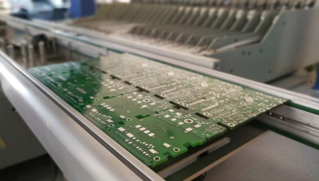
Beyond just size and layers, the complexity of the PCB design also impacts manufacturing costs. Densely populated boards with intricate routing and spacing needs are more expensive to produce.
For example, high component density requires more precision drilling and routing between tightly packed surface mount pads. This increases tooling time and cost. Copper features spaced very closely together also take more care to achieve.
Likewise, designs with loads of tiny vias or high via densities add fabrication steps and expense, especially for blind/buried vias between inner layers. Dense routing with thin trace widths and clearances also adds cost.
High-speed designs require carefully controlled impedance traces and matched lengths. And HDI technologies with microvias are on the pricier end.
Of course, you can’t remove design complexity just to save money if it’s essential to circuit function. But being design-for-manufacturing (DFM) aware and minimizing intricacy where possible helps reduce bare PCB costs.
So component density, routing complexity, small features, and precision needs are key drivers. Evaluating these early provides cost awareness.
The materials used for layers and finishes also drive bare PCB costs. More exotic or high-end materials increase fabrication expenses.
For the board substrate, common choices are FR-4 glass epoxy, high-frequency materials like Rogers, or flexible films. Standard FR-4 is the most cost-effective. High-frequency and flexible materials add cost.
Copper thickness for signal layers impacts cost as well. Thicker copper (2 oz+) improves power transmission but uses more material. 1 oz copper is a common balance of cost and performance.
Solder masks and surface finishes like ENIG, immersion silver, or gold, add processing steps too. A basic green solder mask and HASL finish are the most economical options.
So material selection, while driven by electrical and physical needs, also impacts bare board fabrication pricing. Understanding these tradeoffs allows smart decisions when choosing PCB materials for new designs.
Special Processing
Certain special processing requirements or capabilities also increase bare PCB manufacturing costs.
For example, boards with high layer-to-layer registration precision for the drilling and lamination process require tighter tolerances and process control. This adds cost.
Likewise, controlled impedance boards need tightly tuned trace dimensions and spacing for proper impedance matching. This demands more precision in fabrication.
Boards designed for high-density interconnect (HDI) technology, with tighter lines/spaces, microvias, and thin core layers also require specialized abilities that increase expenses.
Advanced testing like loaded fixture testing, flying probes, or intensive automated optical inspection (AOI) adds cost as well. Basic electrical testing is standard, but advanced inspection and functional testing add steps.
So special fab processes beyond basic PCB construction and testing increase cost. Carefully evaluate if these high-end capabilities are truly needed, and discuss options with your PCB manufacturer.
Testing and Inspection
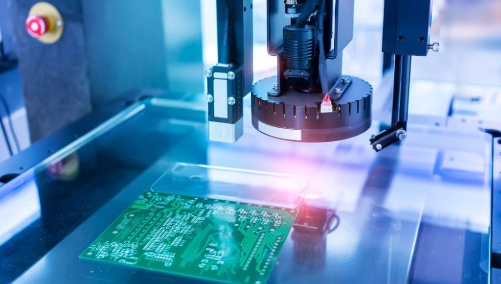
The amount and type of testing and inspection performed on bare PCBs can impact costs as well. More rigorous quality control increases fabrication expenses.
Most PCB suppliers do basic open/short electrical testing on boards as standard procedure. This verifies electrical connectivity but adds little cost.
Additional testing like loaded fixtures or flying probe testing to simulate real-world loading conditions and detect latent defects adds cost. So does intensive AOI to check solder mask and trace defects.
Higher test coverage and more rigorous inspection mean increased quality assurance. But it also increases manufacturing time and expenses.
So teams should evaluate the right balance of test coverage for their program needs. Adding robust testing where needed ensures quality while optimizing costs.
Discussions with your PCB manufacturer on test options can help strike the right balance.
Volume and Lead Time
Order volume also impacts per-unit pricing for bare PCB fabrication. Thanks to economies of scale, higher quantities lead to lower costs per board.
For low-volume prototyping orders, costs are generally higher. But as volumes increase into the hundreds or thousands of boards, bulk discounts kick in and drive down per-unit expenses.
Lead time also plays a role. Rush fabrication with tight turnaround times can increase costs. Standard lead times allow for better scheduling efficiency and cost savings.
So higher volumes paired with standard lead times provide the most opportunity for cost reduction in bare PCB manufacturing. Quantity discounts and production efficiency combine to lower costs.
Coordinate with your PCB supplier on budgetary pricing at estimated order volumes and production timelines. This helps inform early design decisions.
What is PCB Cost Per Square Inch?
Conclusion
The average price of a printed circuit board ranges from $0.02 to $0.05 per square inch. There are dozens of factors that affect the cost of a PCB. The main ones have a linear relationship with costs:
- Board size – Larger boards require more materials, increasing cost per unit.
- Volume – Higher order quantities provide economies of scale, lowering per-unit cost.
- Layer count – Additional layers add materials and processing steps, increasing expense.
- Complexity – More dense component loading and intricate routing adds fabrication costs.
- Component count – Minimizing components reduces materials cost and board real estate needs.
So generally, larger, higher layer count, more complex boards with numerous components will sit at the higher end of the $0.02-$0.05 per square inch cost range. Whereas simpler, smaller boards ordered in high volumes will hit the lower end of the range.
PCB design teams should optimize to balance technical needs and cost requirements. Sourcing specialists can leverage volumes and supplier negotiation to drive down expenses per board. Understanding cost drivers is key to effective budgeting and cost management over a product’s lifecycle.
If you need help reducing bare board PCB manufacturing costs for an upcoming project, the fabrication experts at JHYPCB can advise on design optimization and cost savings. JHYPCB provides low-cost, high-quality PCB fabrication services catered to customer needs. Contact us at sales@pcbjhy.com to discuss your specific requirements.
Related Reading:
- How to Reduce PCB Costs Without Sacrificing Quality
- Building High Quality PCBs – A Comprehensive Guide
- Material selection and performance of multilayer PCBs: how to balance cost and performance
- How to Reduce Manufacturing Costs for Rigid-Flex PCBs?
- High Tg PCB Cost and Pricing: Factors Affecting the Price and How to Save Money
- Affordable PCB Prototyping: Options Worldwide


