Table of Contents
Printed Circuit Boards (PCBs) are critical components widely used in electronic devices. There are different types of PCBs, including single-layer PCBs and double-sided PCBs. Understanding the key differences between single layer and double layer PCBs is crucial, as it directly impacts the design, manufacturing process, and performance of electronic products.
In this comprehensive blog post, we will explore the characteristics, advantages, disadvantages, and applications of both single layer PCBs and double-sided PCBs in detail. We will also provide practical tips and tricks to help you easily identify and distinguish between these two main PCB types for your electronics projects or troubleshooting needs.
What Are PCBs?
A printed circuit board is a flat insulated board that holds and interconnects electronic components using conductive pathways, tracks, or signal traces etched from copper sheets. PCBs serve as the foundation to mechanically support and electrically connect various electronic components in a compact and reliable manner.
The global PCB market was valued at $69.91 billion in 2021 and is projected to reach $89.27 billion by 2028, growing at a healthy CAGR of 4.2% (Source: Prismark Partners LLC). This highlights the crucial role PCBs play across diverse electronic industries and applications.
PCB designs are created using computer-aided design (CAD) software to specify component placement, routing of conductive traces, and board specifications. The PCB manufacturing process involves imaging the circuit patterns onto a copper-clad substrate, etching to remove unwanted copper, drilling holes for component leads, and applying solder mask and silkscreen layers.
No matter how simple or advanced, virtually all electronic devices from household appliances to complex aerospace systems rely on printed circuit boards as the integrated platform to mount and interconnect components reliably and compactly.

Importance of Mastering the Differences between Single Layer and Double Layer PCBs
Mastering the key differences between single layer and double layer PCBs is essential for electronics engineers, designers, and enthusiasts. The ability to distinguish these two fundamental PCB types plays a crucial role in several aspects:
- Optimal PCB Selection: Choosing the right PCB type, single layer or double layer, is vital for efficient circuit design, component placement, and routing. An improper selection can lead to issues like excessive component density, poor signal integrity, electromagnetic interference, and potential product failures.
- Cost Optimization: There is a significant cost difference in the manufacturing of single layer and double layer PCBs. Understanding their distinctions allows cost-effective sourcing decisions based on project requirements and production volumes.
- Performance Implications: Single and double layer PCBs have inherent performance traits that affect parameters like signal speeds, crosstalk, power integrity, and thermal management. Grasping these differences enables designs optimized for the target application’s performance needs.
- Troubleshooting Capabilities: When faced with PCB or product issues, recognizing the PCB type expedites the troubleshooting process by narrowing down potential root causes and failure modes associated with that specific architecture.
Whether designing consumer electronics, industrial equipment, or cutting-edge solutions, a comprehensive grasp of single layer and double layer PCB differences is paramount for electronics professionals aiming to create reliable, cost-effective, and high-performance products.
what are single layer PCBs?
A single layer printed circuit board, often abbreviated as single layer PCB or single-sided PCB, is the most basic and fundamental type of PCB. As the name suggests, it consists of a single layer of conductive material laminated onto an insulating substrate. While the conductive layer is typically copper, there are various single layer PCB types based on different substrate and conductive materials:
- Single Layer Rigid PCBs: These utilize rigid insulating substrates like fiberglass or composite epoxy, with a copper conductive layer. They offer durability and are suited for general applications.
- Single Layer Flexible PCBs: Employing flexible insulating films like polyimide or polyester with a copper layer, they provide bendability ideal for wearables, medical devices, and compact electronics.
- Single Layer Aluminum PCBs: With aluminum as the conductive layer instead of copper, they excel in heat dissipation, making them suitable for power electronics and LED lighting.
- Single Layer Metal-Core PCBs: These feature a conductive metal core like aluminum with an insulating layer and copper traces, combining heat dissipation with higher current capacities.
- Single Layer Ceramic PCBs: Using ceramic substrates like aluminum oxide or aluminum nitride with thick-film conductive layers, they withstand extreme temperatures for harsh environments.
The choice of single layer PCB type depends on factors like cost, application requirements for flexibility, thermal management, high frequencies, or harsh conditions. Despite their simplicity, single layer PCBs cater to a diverse range of needs across industries.

The key characteristics that define single layer PCBs
The key characteristics that define single layer PCBs include:
- Simplicity in Design: With components mounted and interconnected on only one side, single layer PCBs offer a straightforward design approach ideal for basic, low-density circuits.
- Cost-Effectiveness: The simplified single layer construction translates to lower manufacturing costs compared to their multilayer counterparts, making them an economical choice for cost-sensitive projects.
- Lower Component Integration: Due to the single conductive layer constraint, single layer PCBs can accommodate a limited number of components, traces, and interconnections before becoming increasingly complex and congested.
While bearing certain limitations, single layer PCBs remain widely adopted across various applications that prioritize simplicity, cost-effectiveness, and ease of manufacturing over advanced capabilities. Key applications include:
- Basic Consumer Electronics: Simple household devices like remote controls, calculators, and basic gaming accessories often utilize single layer PCBs.
- Hobby Projects & Prototypes: Electronics enthusiasts and makers frequently turn to single layer PCBs for low-cost prototyping and hobbyist projects.
- Legacy System Replacements: Replacements for aging electronics in legacy systems may still incorporate single layer PCBs for compatibility and cost reasons.
According to market research by Technavio, the global single layer rigid PCB market was valued at $4.58 billion in 2020 and is projected to grow at a CAGR of 3.89% from 2021 to 2026, underscoring their continued relevance.
While more advanced multilayer PCBs have superseded many applications, single layer PCBs persist as a fundamental building block in modern electronics manufacturing, catering to specific needs of simplicity, cost optimization, and ease of production.
What are the Characteristics and Features of Single Layer PCBs?
While offering simplicity, single layer PCBs possess several distinct characteristics and features:
- Unilateral Component Placement: With only one conductive layer, all components must be mounted and interconnected on the same side of the board.
- Trace Routing Limitations: The single layer constrains available routing channels for traces, often requiring complicated routes and increased likelihood of signal interference.
- Lower Component Density: The uni-planar design limits the number of components that can be accommodated compared to multilayer counterparts.
- Reduced Design Complexity: The absence of buried or blind vias simplifies the design process for single layer PCBs.
- Cost-Effective Manufacturing: Their basic construction translates to lower manufacturing costs through simpler processes and materials.
- Mechanical Simplicity: Without internal layers, single layer PCBs exhibit higher physical robustness and resilience against delamination.
These traits make single layer PCBs suitable for simple, lower-density circuits where factors like cost-effectiveness, ease of design, and durability take precedence over advanced capabilities.
What are the Advantages and Disadvantages of Single Layer PCBs?
Advantages:
- Economic Choice for Low Complexity Designs
- Simplified Design and Manufacturing Processes
- Mechanical Robustness and Reliability
- Suitable for Prototyping and Low-Volume Production
- Excellent for Simple Circuits and Basic Electronics
Disadvantages:
- Limited Signal Routing and Component Integration
- Signal Integrity Issues Due to Lack of Grounding Planes
- Physical Design Constraints and Space Limitations
- Inability to Handle Complex, High-Speed Circuits
- Thermal Management Challenges with Dense Components
While single layer PCBs excel in simplicity, cost-effectiveness, and ease of design, their inherent limitations make them unsuitable for high-density, high-frequency, or thermally-demanding applications that require advanced multilayer PCB capabilities.
What Are Double Layer PCBs?
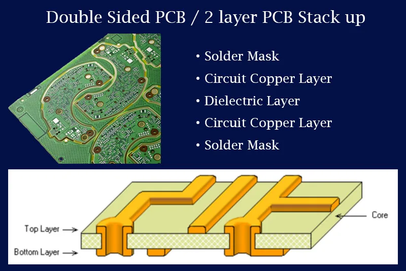
Stepping up from the basic single layer design, double layer PCBs represent an advanced architecture with conductive layers on both sides of an insulating substrate. Also known as double-sided PCBs, they unlock a host of advantages over their single layer counterparts.
The key characteristics of double layer PCBs include:
- Increased Routing Capabilities: With conductive copper layers on both sides, double layer PCBs provide more routing space and channels for complex interconnections between components.
- Higher Component Density: The additional layer allows for denser component population and integration on both sides of the board.
- Incorporated Ground/Power Planes: Double layer PCBs often dedicate one layer as a ground or power plane, enhancing signal integrity, shielding, and power distribution.
- Improved Thermal Management: The ground/power plane can act as a heat-spreading layer, providing better thermal dissipation compared to single layer designs.
- Plated-Through Hole Technology: Double layer PCBs leverage plated-through holes to establish multilayer connections between the top and bottom conductive layers.
According to industry reports, the global double/multi-layer rigid PCB market was valued at $41.92 billion in 2020 and is projected to reach $60.49 billion by 2026, exhibiting a CAGR of 6.4% (Source: QYReports).
While more complex and costlier than single layer PCBs, double layer boards find extensive usage across industries for their ability to accommodate denser circuits, better signal integrity, and improved thermal performance. Key applications span consumer electronics, industrial equipment, automotive systems, and more.
With their versatile capabilities yet balanced complexity, double layer PCBs serve as the mainstream workhorse for modern electronics, bridging the gap between basic single layer and advanced multilayer architectures.
What are the Advantages and disadvantages of using double-sided PCBs?
Advantages of Double Layer PCBs:
- Increased Routing Density and Design Flexibility
- The additional layer provides more routing space for complex interconnections.
- Enables higher component integration and more compact designs.
- Enhanced Signal Integrity
- Dedicated ground/power planes reduce electromagnetic interference.
- Improved shielding and impedance control for high-speed signals.
- Effective Thermal Management
- The ground/power plane acts as a heat dissipation layer.
- Allows for better heat spreading compared to single layer PCBs.
- Higher Current Handling Capabilities
- The extra plane layer provides low resistance current paths.
- Ideal for power electronics and motor control applications.
- Cost-Effectiveness for Medium Complexity
- Balance between single layer simplicity and advanced multilayer boards.
- Optimal for medium density designs without excessive layer costs.
Disadvantages of Double Layer PCBs:
- Limited Design Complexity
- While more capable than single layer, still constrained for high-density/RF designs.
- Complex buried vias and blind vias not possible.
- Susceptibility to Electromagnetic Interference (EMI)
- No dedicated shielding layers like in multilayer PCBs.
- Requires careful layout practices to minimize EMI issues.
- Thermal Dissipation Limitations
- Ground/power plane helps, but limited by lack of dedicated thermal layers.
- High-power component placement requires careful planning.
- Higher Manufacturing Costs than Single Layer
- Additional processing steps for second layer and vias.
- Material costs higher than basic single layer boards.
Comparison of Single Layer and Double Layer PCBs

While single layer and double layer PCBs share some fundamental similarities as printed circuit boards, they exhibit distinct differences that significantly impact their capabilities, applications, and limitations. Here’s a detailed comparison:
- Layer Construction:
- Single Layer PCBs: Feature a single conductive layer (typically copper) laminated on an insulating substrate.
- Double Layer PCBs: Contain two conductive layers, one on each side of the insulating substrate.
- Routing Capabilities:
- Single Layer: Limited routing channels and spaces, leading to complex trace routing and higher signal interference.
- Double Layer: Increased routing density and design flexibility with two conductive layers.
- Component Integration:
- Single Layer: Restricted component placements to one side, resulting in lower density.
- Double Layer: Ability to populate components on both sides, enabling higher component integration.
- Signal Integrity:
- Single Layer: Lack of ground/power planes, leading to potential signal integrity issues.
- Double Layer: Dedicated ground/power plane improves signal quality and electromagnetic shielding.
- Thermal Management:
- Single Layer: Limited heat dissipation capabilities due to single-sided construction.
- Double Layer: Ground/power plane acts as a heat-spreading layer for improved thermal performance.
- Manufacturing Complexity:
- Single Layer: Simpler construction and lower manufacturing costs.
- Double Layer: Additional processing steps for the second layer and plated-through holes, resulting in higher costs.
- Design Constraints:
- Single Layer: Mechanically robust but physically limited in accommodating high-density designs.
- Double Layer: Fewer physical constraints but still limited for highly complex circuits compared to multilayers.
While single layer PCBs excel in simplicity, cost-effectiveness, and suitability for basic circuits, double layer PCBs offer a balanced compromise with enhanced capabilities for medium complexity designs requiring better routing, component density, signal integrity, and thermal performance without the excessive costs of advanced multilayer boards.
Tips and tricks for identifying single layer PCBs and double sided PCBs
Here are some tips and tricks for identifying single-layer PCBs and double-sided PCBs:
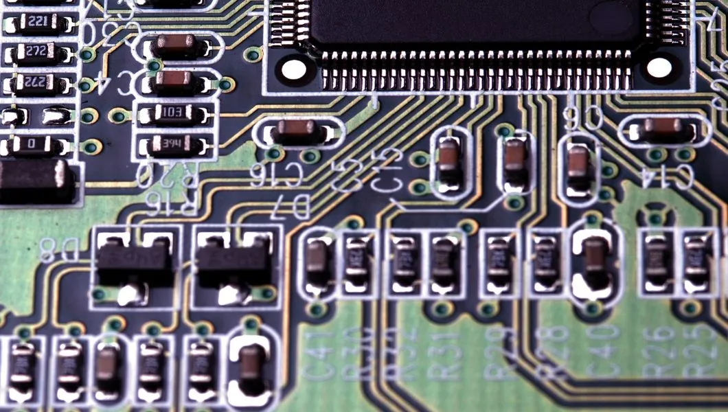
Check for visible solder pads and traces: Single-layer PCBs typically have solder pads and traces on only one side of the board, while double-sided PCBs have them on both sides.
Look for plated-through holes: Double-sided PCBs often have plated-through holes, which allow components to be mounted on both sides of the board.
Inspect the board for vias: Vias are small holes in the PCB that allow for electrical connections between the layers. Double-sided PCBs will typically have vias to connect the top and bottom layers.
Check the surface finish: Single layer PCBs typically have a matte surface finish, while double-sided PCBs may have a glossy finish on one or both sides.
Examine the circuit pattern: Single-layer PCBs will typically have a simpler circuit pattern with fewer components and traces, while double-sided PCBs will have a more complex pattern with a higher density of components.
Check the board thickness: Single layer PCBs are typically thinner than double-sided PCBs due to the use of only one layer of conductive material.
By using these tips and tricks, you can quickly and accurately identify whether a PCB is a single-layer or double-sided board.
Which type of PCB is suitable for different applications
Single layer PCBs and double-sided PCBs have different applications based on their characteristics and features. Here’s an overview of the different applications for each type:
Single-layer PCBs:
- Simple circuits: Single-layer PCBs are ideal for simple circuits that don’t require a high density of components.
- Cost-effective solutions: Single-layer PCBs are a cost-effective solution for low-volume applications and for applications that have low power requirements.
- General-purpose applications: Single-layer PCBs are suitable for a variety of general-purpose applications that don’t require complex circuit designs.
Double-sided PCBs:
- Complex circuits: Double-sided PCBs are ideal for complex circuits that require a high density of components and a large number of interconnections.
- High-performance applications: Double-sided PCBs are suitable for high-performance applications that require reliable signal quality and low noise.
- Compact designs: Double-sided PCBs are commonly used in compact designs that require a small form factor.
When choosing between single-layer PCBs and double-sided PCBs, it’s important to consider the specific requirements of your application. Single layer PCBs are best suited for simple and general-purpose applications, while double-sided PCBs are ideal for complex and high-performance applications. By selecting the right type of PCB for your application, you can ensure optimal performance and reliability.
Here are some examples of products that use single-layer PCBs and double-sided PCBs:
Single-layer PCBs:
- Calculator: Simple electronic devices such as calculators typically use single-layer PCBs.
- LED lighting: LED lights often use single-layer PCBs due to their low power requirements.
- Toys: Many toys and small electronic gadgets use single-layer PCBs due to their cost-effectiveness.
Double-sided PCBs:
- Smartphones: Smartphones use double-sided PCBs to accommodate the large number of components required for advanced functionality.
- Computers: Computers and other complex electronics often use double-sided PCBs due to their ability to accommodate a high density of components.
- Automotive electronics: Modern vehicles use a variety of electronic systems that rely on double-sided PCBs for reliable and high-performance functionality.
These examples demonstrate the versatility and flexibility of single-layer PCBs and double-sided PCBs, and their ability to meet the specific requirements of a wide range of products and applications.
Importance of being able to differentiate between single layer and double sided PCBs
The ability to differentiate between single-layer PCBs and double-sided PCBs is important for several reasons:
Selection of the appropriate type of PCB: By being able to differentiate between single-layer PCBs and double-sided PCBs, you can select the appropriate type of PCB for your electronic project. Choosing the wrong type of PCB can result in issues such as overcrowding of components, which can lead to malfunctions and failure of the device.
Troubleshooting and repair: In the event that an electronic device using a PCB experiences issues, being able to identify the type of PCB can assist in the troubleshooting and repair process. This knowledge can help in the identification of issues related to the PCB, such as broken traces or damaged components.
Understanding of electronics: Being able to differentiate between single-layer PCBs and double-sided PCBs is a fundamental aspect of understanding electronics and how they work. This knowledge can be useful for individuals who want to pursue a career in electronics or for those who are interested in the field as a hobby.
Overall, being able to differentiate between single-layer PCBs and double-sided PCBs is a fundamental skill for anyone who works with electronics or has an interest in the field. This knowledge can help in the selection of the appropriate type of PCB, troubleshooting and repair, and overall understanding of electronics.
Final thoughts and recommendations
In conclusion, understanding the differences between single layer PCBs and double sided PCBs is a crucial aspect of electronics. By knowing the characteristics, features, advantages, and disadvantages of these two types of PCBs, you can make informed decisions in selecting the appropriate type for your project.
When identifying a PCB, it’s important to use a combination of visual cues and a multimeter to ensure accuracy. Additionally, choosing the right type of PCB is essential to the success of your project, as it can impact the functionality and reliability of your electronic device.
Finally, as technology continues to advance, the importance of PCBs in electronics is only set to grow. If you’re interested in electronics or pursuing a career in the field, it’s essential to have a strong understanding of PCBs and their applications.
Overall, I recommend that readers take the time to learn more about single layer PCBs and double sided PCBs, and the role that they play in electronics. Whether you’re an experienced engineer or just starting out, this knowledge will be invaluable as you work on electronic projects and continue to explore the field of electronics.
Conclusion
In summary, this blog post covered the following points related to single-layer PCBs and double-sided PCBs:
- Explanation of what PCBs are and their importance in electronic devices.
- Definition and characteristics of single-layer PCBs, including their simplicity, low cost, and ease of use.
- Definition and characteristics of double-sided PCBs, including their ability to accommodate a high density of components and their higher cost.
- Comparison of the advantages and disadvantages of using single-layer PCBs and double-sided PCBs.
- Tips and tricks for identifying single-layer PCBs and double-sided PCBs, including visual cues and the use of a multimeter.
- Overview of the different applications for single-layer PCBs and double-sided PCBs, and the importance of selecting the appropriate type of PCB for your specific application.
- Examples of products that use single-layer PCBs and double-sided PCBs, include calculators, smartphones, and automotive electronics.
By understanding the characteristics and applications of single-layer PCBs and double-sided PCBs, you can make informed decisions when selecting the appropriate type of PCB for your electronic project.
As a leading PCB manufacturer in China, we have extensive experience in producing high-quality single layer and double sided PCBs for various industries. If you’re in need of reliable PCB solutions, we’d love to discuss your project with you and see how we can help. Contact us today to learn more about our capabilities and services.
Related Reading:
- What are the Single Layer PCB Types?
- Key Considerations for Choosing a Reliable Single-Layer PCB Manufacturer
- The Advantages of Double-Sided PCBs for Prototyping
- How Single-Sided PCBs are Made: An In-Depth Look into the Manufacturing Process
- Double Layer PCB: All You Need To Know About These Specially Printed Circuit Boards
- Speed Up Your PCB Design with Double Sided Prototyping
- The Pros and Cons of Using Double Sided PCBs in Circuit Design
- The Many Uses and Benefits of Double-Sided PCBs
- What Are The Benefits And Applications of Multilayer PCB?
- Rigid PCB vs. Flexible PCB: Which is Right for Your Next Project?
- High Tg PCB vs. Standard PCB: What’s the Difference and Which One to Choose?
- Metal Core PCB vs. FR4: What is the Different?
- What Are The Differences Between HDI PCBs and Traditional PCBs?
- Types of PCBs: Comprehensive Guide to Printed Circuit Boards