As a leading PCB manufacturer in China, JHYPCB has extensive experience designing and producing high-quality heavy copper PCBs for customers worldwide. Increasingly, we have seen growing demand for heavy copper PCBs, which utilize copper trace and plane thicknesses greater than the standard 1oz found on typical PCBs. Common heavy copper PCB weights include 2oz, 3oz, and even up to 6oz or more copper thickness. These heavy copper PCBs offer several key advantages:
- Increased current capacity thanks to the larger cross-sectional area of the thicker copper traces, allowing more amps without overheating.
- Improved heat dissipation as the heavy copper layers spread heat more effectively from high-power components.
- Lower voltage drops across the heavy copper traces and planes that carry substantial current loads.
- Increased mechanical durability and resistance to wear, making heavy copper PCBs ideal for harsh environments.
- Higher tolerance for factors like etching variation and copper fold-over during PCB fabrication.
While providing significant performance benefits, designing reliable heavy copper PCBs requires careful consideration of thermal, electrical, mechanical and manufacturing aspects. In this comprehensive guide, we outline tips for successfully designing heavy copper PCBs that meet demanding current, thermal and durability requirements. JHYPCB’s team has deep expertise in manufacturing robust heavy copper PCBs tailored to our customers’ needs.
What are Heavy Copper PCBs?
The term “heavy copper PCB” refers to printed circuit boards that utilize copper foil weights greater than the standard 1oz (0.035mm or 1.4mils) thickness typically used for most conventional PCB designs. Common heavy copper weights employed in PCB manufacturing include:
- 2oz Copper (0.070mm or 2.8mils)
- 3oz Copper (0.105mm or 4.2mils)
- 4oz Copper (0.140mm or 5.6mils)
- 6oz Copper (0.210mm or 8.4mils)
- And even heavier gauge copper foils beyond 6oz in specialized applications.
These increased copper thicknesses provide several key performance advantages over standard 1oz PCBs:
- Higher Current Carrying Capacity – The larger cross-sectional area allows heavy copper PCB traces to safely handle substantially higher current loads before hitting thermal limits.
- Improved Thermal Dissipation – The thicker copper layers act as enhanced heat spreaders and heat sinks, dissipating thermal loads more effectively from high-power components.
- Lower Voltage Drops – With reduced resistivity, the same heavy copper PCB trace experiences lower IR voltage drops when carrying high currents.
- Increased Mechanical Ruggedness – Heavy copper PCB traces and planes are more resistant to damage from vibration, flexing, accelerated wear and tear.
However, heavy copper PCB designs also introduce additional considerations like managing thermal expansion forces, adjusting manufacturing processes for thicker copper, and potentially higher costs. Careful design optimization is required to leverage the full benefits.
Heavy copper PCBs find extensive usage in harsh-environment applications like automotive, aerospace, industrial controls, RF communications and other industries where reliability and performance are paramount.
In the sections below, we outline comprehensive guidelines for successfully designing heavy copper PCBs…
Heavy Copper PCB Design Steps Guideline
Step 1: Determine where heavy copper PCB layers are needed
The first crucial step in designing a heavy copper PCB is to analyze the circuit and thermal requirements to determine the optimal placement of the thicker copper layers. You want to strategically allocate the heavier copper weights only in areas that will truly benefit, as overusing thick copper throughout can unnecessarily drive up costs and complexity. Some key factors to consider when identifying areas for heavy copper PCB layers:
- High current traces – Any power traces or signal routes that will carry substantial continuous current loads are prime candidates for using heavy copper PCB layers. This includes power rails, motor leads, and other high-power interconnects. The increased cross-section of the thicker copper minimizes resistive losses and heating.
- Heat dissipation – Components like voltage regulators, drivers, processors and other ICs that generate significant heat are ideal for having heavy copper plane layers nearby or directly underneath them. The added copper thickness helps spread and dissipate heat more effectively, preventing hot spots.
- RF/microwave transmission lines – Utilizing heavy copper PCB layers builds low-loss, robust RF and microwave transmission lines, as the skin effect impact is reduced with increased copper thickness.
- Mechanical durability – Areas subject to vibration, repeated insertions/removals, or other physical stresses can benefit from reinforced heavy copper PCB traces and pads for improved durability.
- High voltage – Since voltage drop scales with current, high voltage traces like those feeding vacuum tube amplifiers may require heavy copper PCB layers to minimize IR drops.
Take ample time upfront analyzing current paths and preliminary layouts to identify heavy copper PCB opportunities. Consulting with JHYPCB’s experienced PCB engineers can further pinpoint areas likely to gain performance advantages from thicker copper weights. Careful planning ensures you utilize heavy copper PCB layers strategically where needed without bloating costs unnecessarily.
Step 2: Select the appropriate heavy copper PCB weight
Once you have identified the areas requiring heavier copper for your PCB design, the next critical decision is selecting the ideal copper weight or thickness for those heavy copper PCB layers and traces. Common heavy copper weights used in PCB manufacturing range from 1oz, 2oz, 3oz, up to 6oz and beyond, with each option having pros and cons to consider. Key factors that influence the optimal heavy copper PCB thickness include:
- Current carrying capacity – Doubling the copper weight effectively doubles the current capacity before hitting thermal limits. Calculate the maximum anticipated currents and target below 500 circular mils per amp to ensure adequate margin.
- Thermal performance – Thicker heavy copper PCB layers offer superior thermal capabilities for spreading and dissipating heat away from high-power components. 2oz or 3oz weights are often employed, but extensive thermal modeling may justify 6oz copper or more.
- Manufacturability constraints – As copper weight increases, tolerances tighten and issues like copper fold-over into spaces become more prevalent. Engage with JHYPCB’s engineers to understand manufacturing limitations.
- Cost impact – Heavy copper PCB layers drive up raw material expenses significantly. A 6oz copper PCB could cost 5-10x more than standard 1oz boards, so judicious use is critical.
- Weight considerations – The added mass of thick copper PCB layers may create challenges for lightweight or portable product designs requiring low weight.
- Layer count – With higher PCB layer counts available, copper weight requirements can potentially reduce by utilizing addition innerlayers for power distribution.
- Voltage drop budgets – If tight voltage drop constraints exist, such as powering vacuum tube amplifiers, the maximum available heavy copper PCB weights may be mandated.
The key is striking the right balance between performance and cost by only utilizing the copper weight truly needed in each area of the heavy copper PCB. Often, a strategic mix of different weights like 2oz and 6oz can optimize the design. JHYPCB’s engineers can help model out these tradeoffs.
Step 3: Adjust trace widths for heavy copper PCB layers
Once the heavy copper PCB weights have been established for different areas, the next key step is adjusting the trace width rules accordingly. The larger cross-sectional area of these thicker copper layers allows narrower traces to safely handle the same current load. However, heavier copper weights also necessitate wider minimum trace and space widths to account for tighter fabrication tolerances. Follow these heavy copper PCB design guidelines:
- Width based on current density – Size traces using the 500 circular mils per amp rule, which means a 5A trace only requires 20 mils width in 2oz heavy copper PCB versus 50 mils for 1oz weight.
- Minimum trace/space rules – Adhere to the PCB manufacturer’s specified minimum trace/space design rules, which increase as copper weight goes up. JHYPCB can provide these heavy copper PCB design rules.
- Copper fill considerations – With greater copper cross-section, be aware of increased copper fill that can cause overheating risks on internal layers. Expand spacing between heavy copper PCB traces and planes.
- Solder mask web extensions – Add solder mask web extensions, typically 0.25mm per side, on heavy copper PCB traces carrying high currents to prevent solder wicking.
- Enlarged pad geometry – Increase pad sizes equal to at least the desired heavy copper PCB trace width for components handling high current for reliable solder joints.
- Routing channel fit – Ensure wider heavy copper PCB traces can still fit within routing channels on the board layout without necking down excessively.
- Impedance impacts – Review impedance requirements, as the increased capacitance to ground from thicker traces can impact high-speed signal integrity on the heavy copper PCB.
It is highly recommended to cross-check your heavy copper PCB design rules against the manufacturer’s design rules checker. Don’t assume standard 1oz copper design rules apply. References like IPC-2221 also provide guidance on heavy copper PCB trace sizing.
Step 4: Manage thermal expansion in heavy copper PCB designs
One critical consideration when designing heavy copper PCBs is properly managing the thermal expansion effects from the increased copper weight. As copper thickness increases substantially over standard 1oz PCBs, the difference in expansion and contraction rates with temperature changes also rises. If not addressed, this can lead to various failure modes:
- Pad cratering/lifting – The thick, rigid heavy copper PCB traces can causepadcrater and completely lift pads off the board when severely contracting at extremely low temperatures.
- Delamination – The shear forces generated between the heavy copper PCB layers and other materials with mismatched thermal expansion can delaminate and separate the board layers.
- Trace/via cracking – Rapid localized expansions and contractions can crack the plated through-holes, vias and heavy copper PCB traces themselves.
- Board warping – Uneven thermal expansion forces across different areas of a heavy copper PCB can lead to board warping and structural failures.
Several strategic techniques exist to mitigate these thermal expansion risks in heavy copper PCB designs:
- Intermittent trace design – Break up long, continuous heavy copper PCB traces into intermittent segments with gaps to allow expansion/contraction within each segment.
- Relief gaps and voids – Incorporate carefully placed cut-outs, slashes and voids alongside the high-current heavy copper PCB traces and planes to create expansion relief channels.
- Optimized pad shapes – Utilize rounded, curved pad shapes versus rectangular pads with sharp corners which are more prone to fracturing under thermal stresses.
- Matched material CTEs – Pair the heavy copper layers with materials like Invar that have matching low coefficients of thermal expansion to minimize shear forces.
- Copper-filled reinforcement – Add arrayed copper-filled vias to reinforce and tie the heavy copper PCB layers together while allowing some relative movement.
- Thermal simulations – Use physics-based thermal modeling tools like Ansys to thoroughly simulate and identify high-risk areas requiring mitigation steps.
By designing in robust thermal expansion management from the start, heavy copper PCBs can reliably withstand thermal cycling without failures. Leverage JHYPCB’s expertise in this area for guidance on thermally-reliable heavy copper PCB designs.
Step 5: Include adequate clearances for heavy copper PCB designs
When working with increased copper weights on heavy copper PCBs, it is crucial to include sufficient clearance distances to account for the higher current densities, voltage potentials, and thermal effects. Inadequate clearances can lead to detrimental issues like arcing, insulation breakdown, electromagnetic interference and even safety hazards. Follow these heavy copper PCB design guidelines for clearances:
- High current clearances – Increase the clearance between heavy copper PCB traces/planes carrying high currents over 5A and any other conductors to prevent arcing or insulation breakdown. A minimum 2mm (80mil) clearance is generally recommended.
- Voltage clearances – Adjust clearances based on the expected voltage drops across the heavy copper PCB conductors to maintain adequate isolation margins. A 1V drop may require 5mm versus 2mm for lower voltages.
- Creepage requirements – Check for any modified creepage and clearance requirements that may apply for extraordinarily thick heavy copper PCBs that deviate from standard 1.6mm board thicknesses.
- EMI/EMC separation – Maintain adequate separation distances between high current/voltage heavy copper PCB traces and sensitive components like oscillators to prevent electromagnetic interference.
- Mechanical clearances – Ensure appropriate clearances from chassis walls, fasteners, and any mounted hardware, though slightly reduced margins may be acceptable with more rigid heavy copper PCB designs.
- Mixed copper zones – In boards combining standard and heavy copper PCB layers, ensure the normal 1oz copper clearances are maintained in those areas.
- Arc-chute venting – Account for reduced arc-chute venting on internal heavy copper PCB layers with greater copper fill. Additional cut-outs or vent channels may be required.
Consult IPC standards like IPC-2221 as well as your heavy copper PCB manufacturer’s specific design rules which will depend on parameters like copper weight, intended environment (humidity, pollution) and voltage/current levels. Designing adequate clearances upfront prevents costly PCB field failures.
JHYPCB has extensive experience with heavy copper PCB designs across diverse applications. Our engineering team can support calculating custom clearance requirements and implementing robust designs for your products.
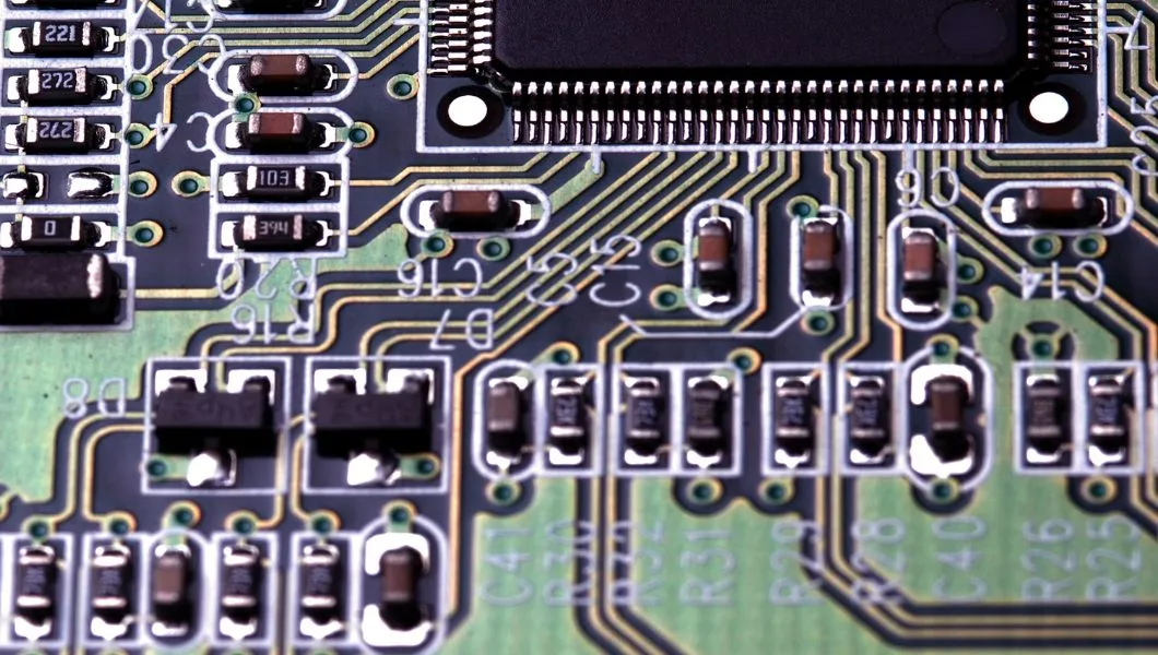
Step 6: Account for manufacturability of heavy copper PCBs
While offering significant performance benefits, designs utilizing heavy copper PCB layers present unique manufacturing challenges that must be carefully considered and accounted for upfront. Heavy copper weights above 2oz push the limits of standard PCB fabrication processes. By working closely with your heavy copper PCB manufacturing partner like JHYPCB, you can ensure your design adheres to established design rules and capabilities. Key manufacturability factors to review include:
- Minimum trace/space design rules – As copper weight increases, so do the minimum trace width and spacing rules to prevent shorts/opens. For example, 6oz copper may require 8mil minimum tracks/gaps versus 5mil for 1oz weight.
- Platedthrough-hole tolerances – With heavy copper PCBs, plated through-hole diameters have much tighter tolerances due to etching variance impacts. This affects pad/hole sizing.
- Copper fold-over prevention – Thick copper conductors are more prone to fold-over defects into adjacent traces or holes during the lamination process. Tight track/hole separations must be avoided.
- PTH barrel fill capability – Properly and evenly filling a 12mil+ PTH barrel with 4oz+ copper requires specialized plating processes and setups from the manufacturer.
- Copper weight variation limits – Be aware of the manufacturer’s line width variation limits which may be higher for extremely heavy copper weight PCB layers.
- Panel utilization impacts – With their increased thickness, heavy copper PCB designs require more panel space reducing available utilization. Ensure required margins.
- Thermal profile compatibility – The high temperature cycles needed to adequately heat and solder thick, heavy copper PCB layers may exceed the limits of some assembly partners.
By proactively collaborating with JHYPCB’s heavy copper PCB manufacturing experts during design, you can avoid costly revisions and respect process constraints. Design rule guidance, stack-up capabilities, fabrication tips and even thermal simulation support are available.
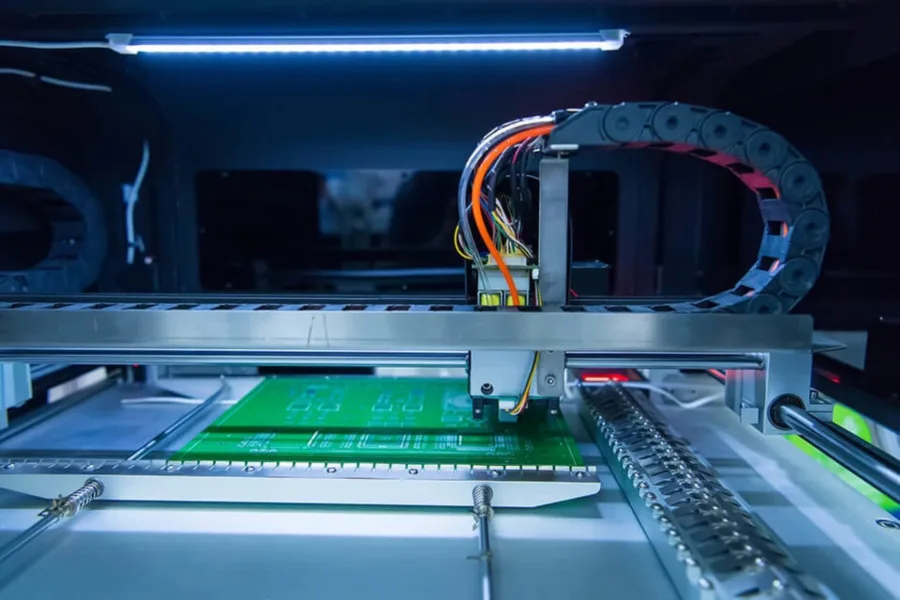
JHYPCB has extensive invested in state-of-the-art heavy copper PCB manufacturing capabilities with specialized plating lines, ovens, and inspection systems to ensure your high-reliability designs are produced flawlessly at any weight and layer count. Our ISO-certified facilities utilize rigorous quality control and IPC compliance.
Step 7: Perform comprehensive thermal analysis for heavy copper PCB designs
Robust thermal simulation and analysis is absolutely critical when designing heavy copper PCBs to ensure reliable performance under extreme temperature conditions. Upfront thermal modeling during the design phase provides invaluable feedback to optimize copper weights, layer stacks and component placement before manufacturing and mitigate potential hot-spot risks. Follow this best-practice workflow for heavy copper PCB thermal analysis:
- Create preliminary heavy copper PCB layout – Build initial board layout identifying copper weight regions, critical components, and board shape/size.
- Construct 3D thermal model – Develop detailed 3D model incorporating actual copper weights, board stackup, component thermal models, and material properties.
- Apply power/load profiles – Set up thermal loads mimicking both peak and continuous operating power profiles for all components and copper planes.
- Simulate across ambient ranges – Run transient and steady-state thermal simulations across expected ambient temperature ranges, accounting for radiation, convection, etc.
- Identify hot spots/violations – Pinpoint areas violating maximum temperature, heat density, or temperature gradient specifications on the heavy copper PCB.
- Iterate copper weight/layout – Adjust copper pour weights, add thermal vias/reliefs, modify cooling channels or tweak component placement to improve temperature distribution.
- Converge on optimal design – Iterate through further thermal simulation cycles until all requirements are reliably met with adequate design margin.
- Sensitivity analysis – Quantify thermal behavior sensitivity to manufacturing variances and boundary condition changes to ensure robust design.
Advanced thermal simulation tools from vendors like Ansys, SolidWorks, SimScale and others are essential for this analysis. JHYPCB partners with leading thermal simulation experts to support our customers’ heavy copper PCB designs.
Upfront investment in thermal modeling prevents costly proto-spins and field failures. JHYPCB’s engineers work closely with your team throughout the thermal simulation process to develop an optimized, reliable heavy copper PCB design from day one.
By following industry best practices for thermal analysis tailored to heavy copper PCB designs, you can extract the maximum performance and lifesspan advantages while mitigating all thermal-related risks. Let JHYPCB’s expertise ensure your success.
conclusion
Heavy copper PCBs provide substantial performance advantages thanks to the thicker copper layers facilitating increased current handling, superior thermal dissipation, reduced voltage drops, and enhanced mechanical durability. However, designing reliable heavy copper PCB solutions require carefully addressing thermal, electrical, mechanical and manufacturing considerations.
In this comprehensive guide, we outlined expert tips for leveraging heavy copper PCBs across the entire design cycle:
- Determining strategic areas for using 2oz, 3oz, 6oz or higher copper weights
- Selecting ideal copper thicknesses based on current, thermal and voltage requirements
- Adjusting trace widths and spacing rules for heavier copper PCB layers
- Managing thermal expansion forces to prevent failures like pad cratering and delamination
- Ensuring adequate clearances between high current/voltage conductors
- Accounting for manufacturability constraints like plating, etching and lamination limits
Rigorous thermal analysis and simulations tailored to heavy copper PCB designs are also imperative to optimize performance, reliability and product lifespan from the start.
As a leading heavy copper PCB manufacturer, JHYPCB has extensive experience partnering with customers on thermally-reliable, high-current designs across industries like automotive, aerospace, industrial equipment and more. Our advanced heavy copper PCB manufacturing capabilities combined with simulation and engineering expertise allow us to be your turnkey partner.
Contact JHYPCB today to discuss your upcoming heavy copper PCB project requirements. Our team is ready to provide guidance from concept to prototype to high-volume production, ensuring a successful and optimized design. Let’s leverage the full advantages of heavy copper PCBs together!