Printed circuit boards serve as the foundation for almost all modern electronics. They provide the mechanical structure and electrical connections that allow components to be assembled into functioning circuits and systems. As electronic devices and systems handle increasing levels of power and become more complex, this puts greater demands on the capabilities of the PCBs. This is leading to rapid growth in the use of heavy copper PCBs.
Heavy copper PCBs contain thicker copper layers compared to standard 1oz copper PCBs. While 1oz copper has a thickness of around 35 microns, heavy copper PCBs use copper at 2oz, 3oz, 4oz, or even higher. This equates to copper thickness in the range of 70 microns up to 280 microns or more.
The key benefits provided by the thicker copper are higher current carrying capacity, better thermal dissipation, and improved reliability under temperature cycling or vibration loads. Heavy copper PCBs can handle substantially higher currents compared to standard-thickness copper, with lower voltage drop and less heating. The thicker copper also acts as a heat spreader, conducting heat efficiently away from hot spots on the PCB. This is essential for managing the thermal loads from high-power devices.
With their unique electrical and thermal properties, heavy copper PCBs are becoming indispensable in a wide range of high-power and performance-critical applications. These include power electronics such as inverters, converters, and motor drives, LED lighting, automotive electronics, industrial motor controls, telecom/datacom equipment, and more. As demands for higher power densities, miniaturization, and reliability grow, heavy copper PCBs will take on an increasingly crucial role.
Applications and Benefits of Heavy Copper PCBs
Heavy copper PCBs provide substantial performance advantages that make them the ideal choice for a wide range of high-power and high-reliability applications. Let’s look at some of the key uses and benefits.
In the field of power electronics, heavy copper enables efficient operation of devices like inverters, converters, and motor drives. These devices switch and control high currents. The thick copper can carry current spikes without excessive heating or voltage drops. This allows the electronics to handle higher power levels within the same footprint.
For LED lighting, especially high-power LEDs, heavy copper is invaluable. The thick copper layers act as a heat spreader. This dissipates the heat from the tightly packed LEDs, preventing hot spots. By managing heat effectively, heavy copper PCBs enable brighter, more efficient, and more reliable LED lighting.
Automotive applications such as EV charging systems, inverters, sensors, and control units must withstand vibration, shocks, and temperature swings. Heavy copper PCBs possess the mechanical sturdiness and reliability under thermal cycling to meet automotive demands. Hybrid and electric vehicles in particular benefit from the high currents and superior cooling abilities of heavy copper.
In industrial equipment like motor drives, robotics, and CNC machines, heavy copper provides the ruggedness to endure vibration, contamination, and repeated temperature changes. The PCBs can carry the high currents needed for precision equipment and shorten electrical paths for quick response times.
For telecom and datacom hardware like routers, switches, servers, and base stations, heavy copper offers a solution to rising thermal loads. It conducts heat away from densely packed ICs and high-speed interfaces, preventing overheating of sensitive electronics. This supports the reliable operation of communication infrastructure.

Technology Overview of Heavy Copper PCB
Now let’s look at some of the key terminology and manufacturing processes related to heavy copper PCBs. This will provide a better understanding of the technology.
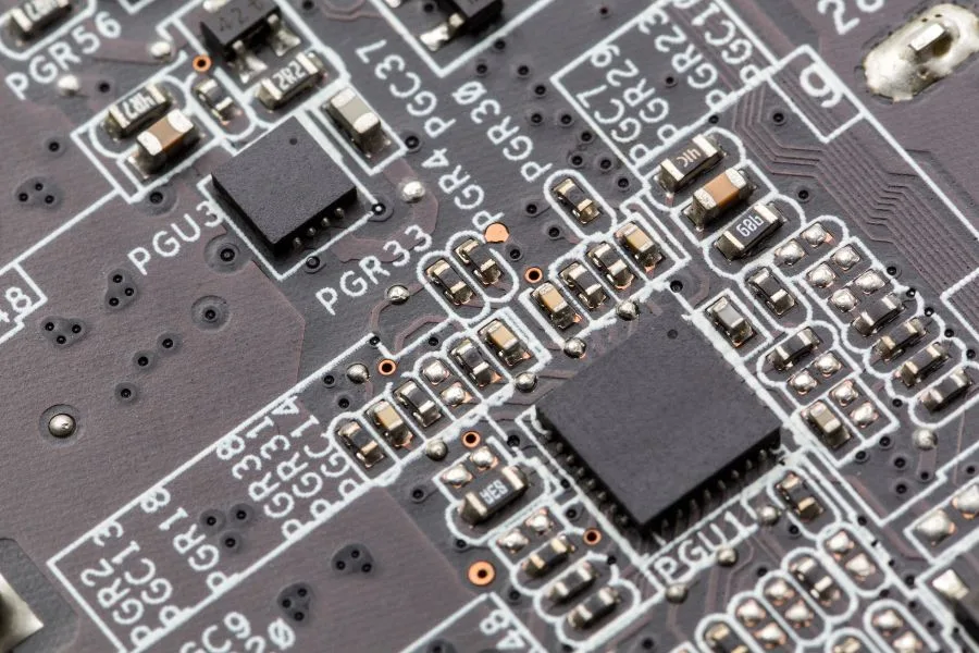
First, “heavy copper” refers to the thickness of the copper foil used in the PCB. Common heavy copper weights are 2 oz (70 μm), 3 oz (105 μm), 4 oz (140 μm) and so on. The heavier the copper foil, the thicker it is. This contrasts with standard 1 oz (35 μm) foil used on regular PCBs.
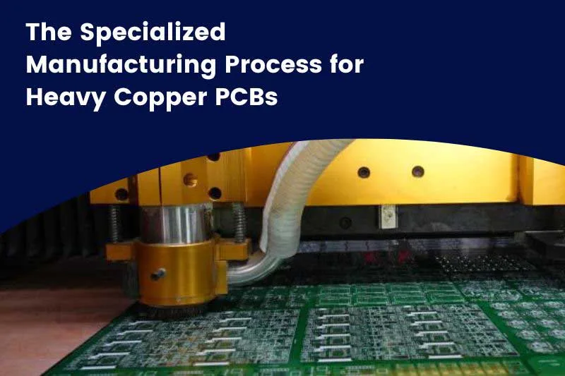
To fabricate heavy copper PCBs, special plating processes are used. Panel plating involves plating up the entire copper surface to build up thickness. Pattern plating localizes the thick copper only in certain areas. This conserves copper where it’s not needed.
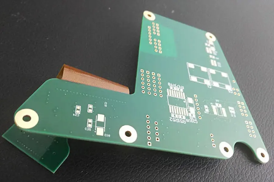
An important design consideration is trace and gap dimensions. Similar widths and clearances must be maintained despite the thicker copper. Careful trace routing enables proper thermal management on heavy copper PCBs.
Drilling and hole walls also require special attention. High-precision drilling is needed to achieve the tighter tolerances required. Plated through holes must have sufficient copper thickness to withstand thermal cycling.
Special surface finishes may be applied to heavy copper PCBs. These protect against oxidation and provide solderability while withstanding higher temperatures. Common finishes include ENIG, Imm Ag, OSP, and others.
With an understanding of the key terminology and manufacturing processes, it becomes clearer how heavy copper PCBs get their unique properties. This technology knowledge enables the designing of boards optimized for high power and reliability.

Case Studies of Heavy Copper PCB Applications
To illustrate the benefits of Heavy Copper PCBs in real-world applications, let’s look at some case studies:
- Electric Vehicle (EV) Charging Station
EV charging stations require high-power DC charging to minimize charging time. Heavy Copper PCBs can handle high currents and provide efficient thermal management, making them an ideal choice for EV charging stations. A case study showed that Heavy Copper PCBs increased the charging power by 25% compared to conventional PCBs, reducing the charging time by 20%.
- Industrial Automation System
An industrial automation system requires high current carrying capacity and reliable performance in harsh environments. A case study showed that Heavy Copper PCBs provided 50% higher current carrying capacity and improved thermal management, resulting in a more reliable and efficient system.

Trends and Future Outlook of Heavy Copper PCBs
Heavy copper PCB technology will continue advancing to meet growing demands for higher power densities, faster speeds, and greater reliability. Let’s look at some of the key trends driving the adoption of heavy copper PCBs.
Market researchers forecast rapid growth in demand for heavy copper PCBs over the next 5-10 years. This is driven by expansion in applications like electric vehicles, renewable energy, LED lighting, and 5G telecom infrastructure. These all require managing high currents and thermal loads.
Electric vehicles in particular are a massive market for heavy copper PCBs. EVs contain many copper-intensive electronics like inverters, charging systems, and power distribution networks. Some estimate EV adoption could quadruple copper usage in cars.
In consumer devices, heavy copper enables keeping pace with faster processors, more sensors, wireless charging, and other advancing functionality. This maintains reliability as complexity rises.
Experts predict maximum current densities in PCBs could reach up to 35A/mm2 in coming generations. This is driving increased separation between conductors and further adoption of heavy copper for thermal dissipation.
Advances in fabrication are also expanding heavy copper capabilities. This includes pattern plating techniques to reduce costs by placing thick copper only where needed. Enhanced drilling methods allow the production of smaller vias on heavy copper boards.
In summary, the performance demands of modern electronics will spur innovation in heavy copper PCB technology. This will enable continuing gains in power densities, efficiency, functionality, and reliability.

Conclusion
Heavy copper PCBs provide invaluable benefits for high-power, high-speed, and high-reliability electronic systems. To recap, the key advantages of heavy copper are:
- Increased current carrying capacity compared to standard 1oz copper PCBs. This enables handling higher power levels.
- Superior thermal dissipation and heat spreading due to the thicker copper. Essential for managing heat from densely packed components.
- Improved reliability under mechanical stress and temperature cycling. Critical for automotive, aerospace, and military applications.
- The lower voltage drop across traces allows for maintaining signal integrity at high frequencies and currents.
- Enhanced efficiency of power electronic circuits thanks to lower conductive losses in the thick copper.
With demands continuously growing for smaller, faster, more powerful, and more reliable electronics – heavy copper PCBs will take on an increasingly important role. Their capabilities make them indispensable for leading-edge applications from electric vehicles to data centers powering the cloud.
As heavy copper PCB technology progresses to offer finer features and fabrication advances, it will open doors to next-generation electronics. Innovations in heavy copper will help drive progress across a diverse range of industries.