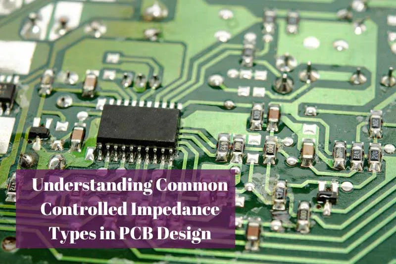
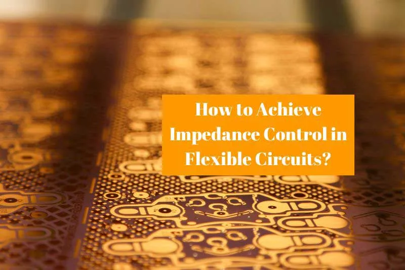
Flexible printed circuits (FPCs) are a unique class of PCBs that can bend and flex to fit challenging form factors. As flexible circuits find increased use in products like wearables, Internet of Things devices, and medical electronics, the demands for performance are rising. These flexible boards are expected to support higher speed signals while withstanding repeated dynamic bending. This requires maintaining good signal integrity through controlled impedance designs.
Impedance control is critical for flex circuits to function properly at high frequencies. When signals propagate down a trace, they expect to see a consistent characteristic impedance. However, impedance discontinuities caused by changes in trace width, dielectric thickness, or bending can reflect signals. These reflections act like echoes, distorting and corrupting the data transmission. Uncontrolled impedance leads to slower rise times, increased electromagnetic interference (EMI), and timing issues. It can even cause functional failures.
By tuning the physical dimensions and materials used in the flexible PCB stackup, designers can engineer controlled impedance signal paths. This allows high-speed signals to transmit cleanly without reflections. Factors like trace geometry, dielectric thickness, layer stackups, and modeling the dynamic bending all come into play when optimizing impedance on flex circuits. With careful design, flexible PCBs can reliably support emerging applications demanding miniaturization, high density, and performance—all without sacrificing signal integrity.
The factors affecting impedance control in flexible circuits
Impedance control in flexible circuits is affected by multiple factors that are closely related.
1. Choice of materials:
- Different materials have different dielectric constants and loss tangents, which affect the circuit’s impedance. For instance, polyimide has a lower dielectric constant than polyetherimide, making it a better choice for high-frequency applications.
- According to a study published in IEEE Transactions on Components, Packaging, and Manufacturing Technology, the choice of substrate material can significantly impact the characteristic impedance of the circuit. The study found that the use of a low-loss dielectric material, such as a ceramic-filled PTFE material, resulted in a lower characteristic impedance compared to other materials.
2. Metal thickness:
- The thickness of the metal traces affects the width and height of the conductors, which in turn affects the impedance value.
- A study conducted by the University of California, Berkeley found that thinner metal traces can result in lower characteristic impedance values. The study also found that narrower trace spacing reduced the parasitic capacitance and inductance, leading to a more consistent impedance.
3. Signal frequency:
- As the signal frequency increases, the requirements for impedance control become more stringent, requiring thinner trace widths and thinner dielectric layers.
- According to a study published in the Journal of Electronic Packaging, the effect of frequency on the impedance of a flexible circuit can be significant, with the characteristic impedance decreasing as the frequency increases.
4. Trace width and spacing:
- The proportion of trace width to spacing determines the impedance value, making it crucial to design these dimensions carefully for impedance control.
- A study published in the Journal of Micromechanics and Microengineering found that varying the trace width and spacing could result in a range of characteristic impedance values, with narrower trace widths and smaller spacing resulting in lower impedance values.
5. Interface structure:
- The interface structure, such as through-hole connectors or open-pin connectors, can affect impedance control.
- According to a study published in the International Journal of Materials Engineering Innovation, the use of through-hole connectors resulted in a higher characteristic impedance compared to surface-mount connectors due to the change in the trace width and thickness around the connector.
6. Manufacturing process:
- The manufacturing process has a significant impact on impedance control, with trace width and thickness control, metal foil attachment, and thickness critical for ensuring consistent impedance.
- A study published in the Journal of Microelectromechanical Systems found that laser ablation was an effective method for achieving precise trace width and thickness control in flexible circuits, resulting in improved impedance control.
7. Layering method:
- The layering method can also impact impedance control, with the stacking arrangement of multi-layer flexible circuits affecting the relative position and spacing of each layer.
- A study published in the IEEE Transactions on Components, Packaging, and Manufacturing Technology found that the use of staggered vias in multi-layer flexible circuits improved impedance control by reducing the coupling between adjacent layers.
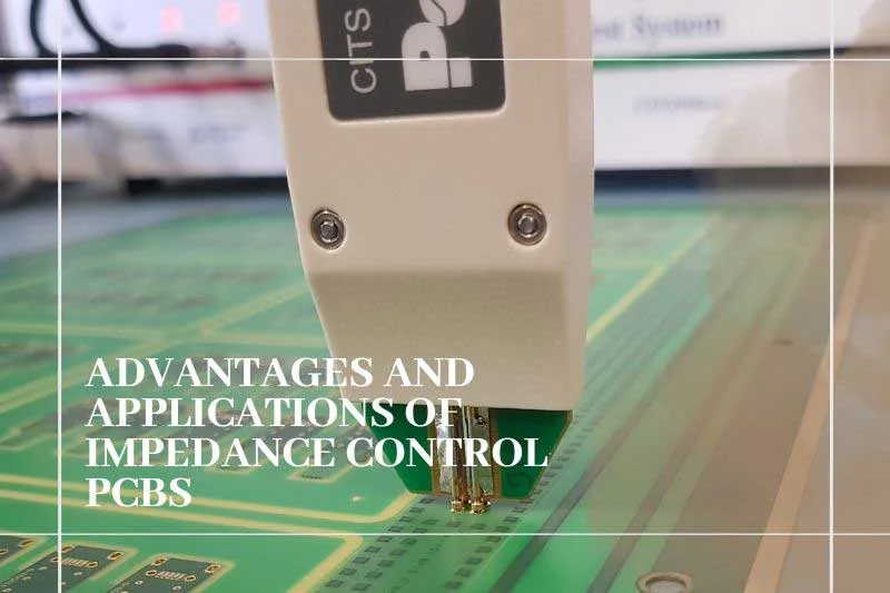
Impedance control strategies for flexible PCBs
- Use impedance-tolerant connections between rigid and flex sections
The interface between rigid boards and flexible circuits can cause impedance discontinuities. Using connectors designed for impedance tolerance smooths this transition. Interconnects like bellows contact or pogo pins maintain conductor spacing and cross-section for consistency. - Maintain consistent dielectric thickness across flex layers
Variations in dielectric thickness will directly impact impedance. Keeping the dielectric layers, bond plies, and cover layers a uniform thickness controls capacitance and impedance. Consistent laminations avoid sudden changes. - Model effects of bending on impedance
Modeling helps predict how dynamic bending impacts impedance. Different bend radii alter conductor spacing and dielectric constants. Simulation provides insight on the effects on impedance over specific bend profiles. - Use plane layers for impedance reference
Adding ground or power planes provides an impedance reference to maintain control. The planes also help reduce EMI and cross-talk. Staggering planes above and below traces establishes a capacitive sandwich. - Minimize length differences in differential pairs
Matching the lengths of differential traces controls impedance and propagation delay. Even sub-millimeter differences can cause data skew. Keeping paired signals symmetrical maintains balance. - Carefully match trace widths to achieve the target impedance
Tuning trace widths is key for dialing in impedance. Follow modeling results to hit the right geometry. Remember wider lines have lower impedance than thinner traces. - Utilize crosshatch ground planes
A grid of orthogonal reference planes above and below traces establishes controlled impedance. The crosshatch planes also reduce EMI. - Use lower-loss dielectric materials like polyimide
Low-loss polymers help maintain signal integrity under bending. Polyimide films have lower dissipation than adhesive dielectrics, especially with high frequencies. - Consider the effects of dynamic flexing during use
Analyze impedance under real-world bending conditions. The radii of flexing points and flex life impact impedance over time.
How Can We Help you?
Are you in need of high-quality and reliable PCBs for your business? Look no further! Our experienced team of experts at JHYPCB is dedicated to providing you with top-notch PCB manufacturing services that meet your specific requirements.
We utilize state-of-the-art technology and the latest manufacturing techniques to ensure that your PCBs are of the highest quality and reliability. With our fast turnaround times and competitive pricing, you can trust us to deliver your PCBs on time and within your budget.
Contact us today to learn more about how we can help you with your PCB manufacturing needs. Let us be your trusted partner in PCB manufacturing and take your business to the next level.
Related Reading: