Introduction
Flex PCB with Stiffener: A Key Component in Modern Electronics
Flexible Printed Circuit Boards are an essential part of modern electronics, offering space, weight, and flexibility advantages. Flex PCBs have gained popularity in various industries, including automotive, medical, military, and aerospace. A stiffener to a Flex PCB provides additional support and rigidity while maintaining the circuit’s flexibility.
This article will introduce Flex PCB with stiffener, defining the concept and highlighting its importance in modern electronics. We will also provide an overview of the manufacturing process, outlining the steps in producing a high-quality Flex PCB with a stiffener. By the end of this article, you will better understand Flex PCB with stiffener and the manufacturing process involved in producing it.
What is Flex PCB?
Flex PCB is an electronic circuit board made of thin, flexible plastic material such as polyimide or polyester. Flex PCBs are designed to be flexible and can be bent, folded, or twisted to fit into tight spaces or conform to irregular shapes, making them ideal for use in products where space and weight are a concern.
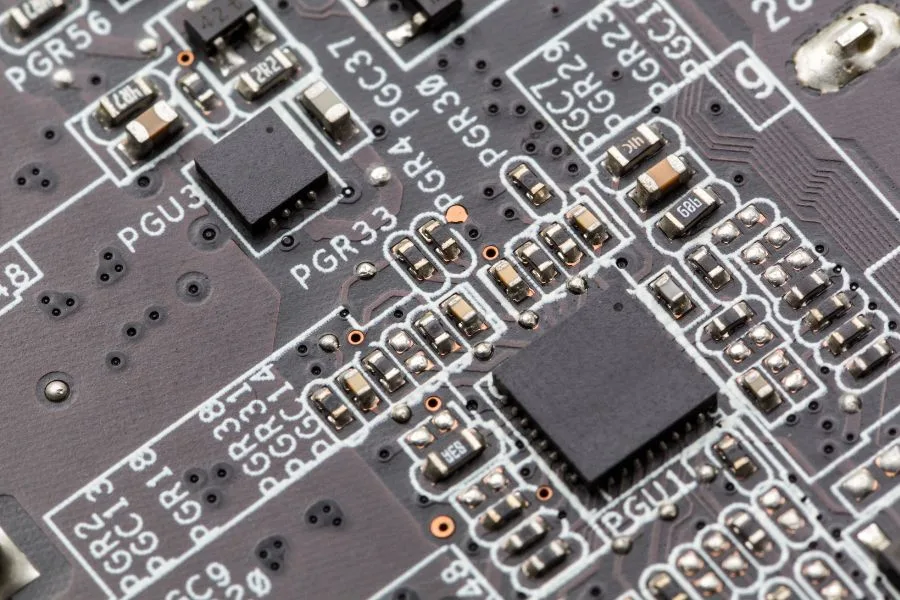
Flex PCBs consist of multiple layers of conductive material, such as copper, separated by insulating layers. These layers are connected through small holes called vias, allowing electrical signals to pass through the board.
Flex PCBs are commonly used in various industries, including automotive, aerospace, medical, and consumer electronics, due to their ability to reduce the size and weight of electronic devices while also increasing their reliability and durability.
What is Flex PCB With Stiffener?
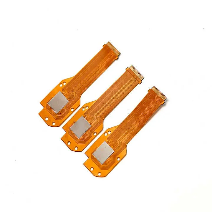
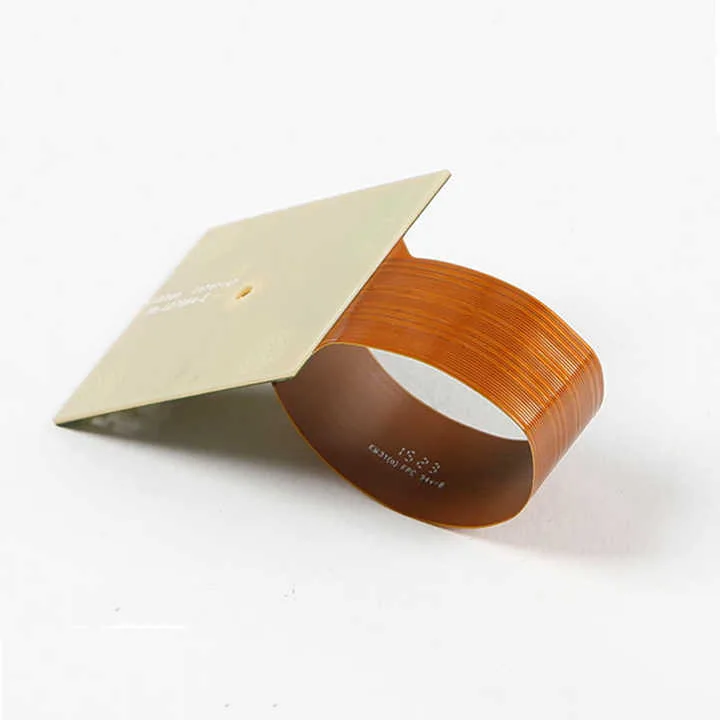
A Flex PCB with a stiffener is a type of printed circuit board designed to be flexible but also incorporates a stiffening element to provide additional support and rigidity in certain areas of the board.
The flexible portion of the PCB is typically made of a thin, flexible substrate material such as polyimide or polyester. This flexible material allows the PCB to bend or conform to a specific shape or contour, making it ideal for use in applications where space is limited or where the PCB needs to be able to bend or flex without breaking.
However, additional support and rigidity may be needed in some areas of the PCB. This is where a stiffener comes in. The stiffener is typically made of a rigid material such as FR4 or aluminum. It is bonded to the flexible portion of the PCB in specific areas where extra support is required. This can include areas around components or connectors where repeated bending or flexing may cause stress on the PCB.
By combining the flexibility of a Flex PCB with the added support of a stiffener, designers can create a flexible and rigid PCB in the right places, allowing for more design flexibility and improved reliability in a wide range of applications.
Designing a Flex PCB with Stiffener
Designing a Flex PCB with a stiffener involves several key steps, including:
Understanding the requirements of the circuit: The first step in designing a Flex PCB with a stiffener is to understand the requirements of the circuit. This includes identifying the components that will be used, the size and shape of the board, and any specific mechanical or electrical requirements.
Determining the number of layers needed: Once the requirements of the circuit are understood, the designer needs to determine the number of layers that will be needed for the PCB. This will depend on the complexity of the circuit and the number of components that need to be placed on the board.
Selecting the substrate material: The substrate material is a key factor in the performance and reliability of the Flex PCB. Common materials used for Flex PCBs include polyimide, polyester, and liquid crystal polymer (LCP). The designer needs to select a flexible material to meet the application’s requirements while also providing the necessary electrical and mechanical properties.
Creating the design layout: Once the substrate material is selected, the designer can begin creating the layout of the Flex PCB. This involves placing the components on the board, routing the traces, and determining the location and shape of the stiffener. The layout must be carefully designed to ensure that the Flex PCB meets all of the requirements of the circuit while also accommodating the stiffener in the appropriate locations.
Adding the stiffener to the design: Once the layout is complete, the designer can add the stiffener to the design. The stiffener is typically placed on the backside of the Flex PCB and bonded to the flexible material in specific areas where additional support is needed. The stiffener can be made from various materials, including FR4, aluminum, or steel, depending on the application’s specific requirements.
In addition to these key steps, designing a Flex PCB with a stiffener requires careful consideration of factors such as thermal management, signal integrity, and manufacturability. By following best practices and working closely with a qualified Flex PCB manufacturer, designers can create high-quality Flex PCBs with stiffeners that meet the unique requirements of their applications.
Preparing the Substrate Material
Preparing the substrate material is an important step in the manufacturing of a Flex PCB with a stiffener. This involves several key steps, including:
Cleaning and preparing the substrate material: The first step in preparing the substrate material is to clean and prepare it for the subsequent layers. This may involve cleaning the surface with solvents, plasma treatments, or other methods to ensure that it is free of dust, dirt, and other contaminants that could affect the adhesion of the subsequent layers.
Applying the adhesive layer: The next step is to apply an adhesive layer to the substrate material. The adhesive layer is typically made from a thermoset or thermoplastic material that can bond the layers of the Flex PCB together. The adhesive layer is applied using a laminator or other equipment that evenly distributes the adhesive across the substrate.
Applying the conductive layer: Once the adhesive layer is applied, the conductive layer is added to the substrate material. Using heat and pressure, the conductive layer is typically made from copper laminated onto the adhesive layer. The copper layer is patterned to create the necessary traces and pads for the circuit.
Applying the protective layer: After applying the conductive layer, a protective layer is added to the substrate material. This layer is typically made from a polyimide film or other material that can protect the circuit from mechanical and environmental stresses. Heat and pressure also laminated The protective layer onto the substrate material.
Applying the stiffener layer: The stiffener layer is applied to the substrate material. The stiffener layer is typically made from a rigid material such as FR4, aluminum, or steel. The stiffener layer is bonded to the substrate material in specific areas where additional support is needed, using an adhesive layer or other bonding method.
Once all the layers are applied to the substrate material, the Flex PCB with stiffener can be processed through the remaining manufacturing steps, including drilling, plating, solder mask application, and component assembly. By carefully preparing the substrate material, designers can ensure that the Flex PCB with stiffener meets the application’s requirements and delivers reliable performance.
Etching the Conductive Layer
Etching the conductive layer is an important step in manufacturing a Flex PCB with a stiffener. This involves several key steps, including:
Applying the photoresist layer: The first step in etching the conductive layer is to apply a photoresist layer to the copper surface. The photoresist is typically a light-sensitive material that can be selectively removed in certain areas to create the necessary traces and pads for the circuit. The photoresist layer is applied using a coating machine or other equipment that evenly distributes the material across the copper surface.
Exposing the photoresist to UV light: Once the photoresist layer is applied, it is exposed to UV light in specific areas using a photomask or other exposure tool. The photomask is a stencil-like pattern that defines the areas where the copper will be removed during the etching process. The UV light causes a chemical reaction in the photoresist layer, which makes it either soluble or insoluble in the developing solution.
Developing the photoresist: After the photoresist layer is exposed to UV light, it is developed using a developing solution. The developing solution removes the photoresist in areas exposed to UV light, leaving the copper surface exposed. The developing solution is typically an alkaline solution that can dissolve the soluble portions of the photoresist layer.
Etching the exposed copper: The final step in the etching process is to etch the exposed copper using an etchant solution. The etchant solution is typically an acidic solution that can selectively dissolve the copper in areas where it is exposed. The etchant solution is applied to the copper surface using a spray or immersion process, and the etching process is closely monitored to ensure that the desired trace and pad geometries are achieved.
Once the etching process is complete, the photoresist layer is removed using a stripping solution, leaving behind the desired traces and pads on the copper surface. By carefully controlling the etching process, designers can ensure that the Flex PCB with stiffener meets the application’s requirements and delivers reliable performance.
Drilling and Plating
Drilling and plating are important steps in manufacturing a Flex PCB with a stiffener. This involves several key steps, including:
Drilling holes for vias and through-holes: The first step in drilling and plating is to drill holes in the copper surface of the Flex PCB for vias and through-holes. Vias are small holes that allow electrical connections between different circuit layers, while through holes are larger holes that allow components to be mounted on the circuit. The holes are drilled using a drilling machine with specialized bits that can create the necessary hole geometries.
Plating the holes with copper: Once drilled, they are plated with copper to create electrical connections. The plating process involves depositing a thin layer of copper onto the walls of the holes using an electroplating process. The copper plating is necessary to create a conductive pathway between the different layers of the circuit and between the components and the circuit.
The plating process typically involves several steps, including cleaning the holes, activating the surface with a solution of palladium and tin, and electroplating the copper onto the surface using a plating solution. The electroplating process is closely monitored to ensure the desired thickness and uniformity of the copper layer.
Once the plating process is complete, the Flex PCB with stiffener can be processed through the remaining manufacturing steps, including solder mask application and component assembly. By carefully drilling and plating the holes, designers can ensure that the Flex PCB with stiffener meets the application’s requirements and delivers reliable performance.
Adding the Stiffener
Adding a stiffener is an important step in manufacturing a Flex PCB with a stiffener. This involves several key steps, including:
Applying adhesive to the stiffener material: The first step in adding a stiffener is to apply adhesive to the stiffener material. The adhesive is typically a heat-curable epoxy that binds the stiffener to the Flex PCB. The adhesive is applied to the stiffener material using a coating machine or other equipment that evenly distributes the material across the surface.
Aligning the stiffener with the Flex PCB: Once the adhesive is applied, it is carefully aligned with the Flex PCB. The alignment process is critical to ensure the stiffener is correctly positioned and will provide the necessary support for the Flex PCB. The alignment process can be carried out manually or using automated equipment, depending on the complexity of the design and the manufacturing process.
Applying heat and pressure to bond the stiffener to the Flex PCB: Once the stiffener is aligned with the Flex PCB, it is bonded to the PCB using heat and pressure. The bonding process typically involves placing the assembly into a heated press that can apply the necessary pressure to ensure a strong bond between the stiffener and the Flex PCB. The assembly is heated to activate the adhesive and allow it to cure, forming a strong bond between the two materials.
Finishing the Flex PCB
Finishing the Flex PCB is an important step in the manufacturing process, which involves several key steps, including:
Applying the solder mask layer: The first step in finishing the Flex PCB is to apply the solder mask layer. The solder mask is a layer of protective material applied to the Flex PCB’s surface to prevent the solder from sticking to areas where it is not intended. The solder mask is typically applied using a screen printing process and can be a variety of colors.
Applying the surface finish layer: The next step is to apply the surface finish layer to the copper surfaces of the Flex PCB. The surface finish layer is a thin layer of metal applied to the copper surfaces to protect them from oxidation and provide a smooth, uniform surface for component attachment. Common surface finishes include HASL (Hot Air Solder Leveling), ENIG (Electroless Nickel Immersion Gold), and OSP (Organic Solderability Preservatives).
Final testing and inspection: The Flex PCB is ready for final testing and inspection once the solder mask and surface finish layers are applied. This typically involves a range of electrical and functional tests to ensure that the circuit is operating correctly and meets the design specifications. The Flex PCB is also inspected visually to ensure that it is free of defects and meets the application requirements.
Once the testing and inspection process is complete, the Flex PCB is ready for deployment in the application. By carefully finishing the Flex PCB, designers can ensure that it meets the application’s requirements and delivers reliable performance, even in challenging operating conditions.
The biggest difference between manufacturing a flexible PCB (Flex PCB) and a rigid PCB
The biggest difference between manufacturing a flexible PCB and a rigid PCB is the flexibility of the substrate material. Flex PCBs require special handling and processing techniques because the flexible substrate material is made from thin, lightweight materials such as polyimide or polyester film. The key differences between manufacturing a Flex PCB and a rigid PCB are as follows:
Substrate material: The substrate material for a Flex PCB is flexible and thin, while a rigid PCB uses a rigid substrate material such as fiberglass or epoxy. The flexible substrate material is typically a polyimide or polyester film, requiring special handling during manufacturing.
Layer stack-up: The layer stack-up for a Flex PCB is designed to allow for flexibility and bending. Flex PCBs are typically composed of several layers of flexible materials, while rigid PCBs have single or multiple rigid layers that are bonded together.
Manufacturing process: The manufacturing process for a Flex PCB is different from that of a rigid PCB. Flex PCBs require special handling and processing techniques to accommodate the flexible substrate material. For example, the substrate material must be rolled, cut, and bonded to create the desired shape and flexibility.
Etching process: The etching process for a Flex PCB is similar to that of a rigid PCB, but the flexible substrate material requires additional care. The substrate material must be flat during the etching process to properly form the traces and features.
The biggest difference between manufacturing a Flex PCB and a rigid PCB is the flexible substrate material. The flexible substrate material requires special handling and processing techniques, making the manufacturing process more complex and time-consuming. However, the flexibility and adaptability of Flex PCBs make them ideal for many applications where rigid PCBs are not suitable.
Conclusion
In conclusion, a high-quality manufacturing process is crucial for creating a reliable and durable Flex PCB with a stiffener. The manufacturing process must consider the substrate material’s flexibility, the design requirements, and the bonding process of the stiffener material. Any defects or inconsistencies in the manufacturing process can lead to failure or decreased performance of the Flex PCB with stiffener.
The future of Flex PCB manufacturing with stiffeners is promising as the demand for flexible and adaptable electronics continues to grow. With technological advancements and manufacturing processes, Flex PCBs with stiffeners can be designed and produced with higher precision, speed, and cost-effectiveness. Using new materials, such as flexible 3D-printed substrates, may also expand the possibilities for Flex PCBs with stiffeners in the future. As such, manufacturers must stay up-to-date with the latest technologies and production techniques to continue meeting the needs of the ever-evolving electronics industry.
Looking for a trusted and experienced Flex PCB manufacturer? JHYPCB offers a range of flexible circuit solutions, including single-sided, double-sided, and multi-layer Flex PCBs and Flex PCBs with stiffeners. Our commitment to quality and attention to detail ensures that your circuits are manufactured to the highest standards. Contact us today at sales@pcbjhy.com to discuss your project requirements and get started on your flexible circuit journey!