
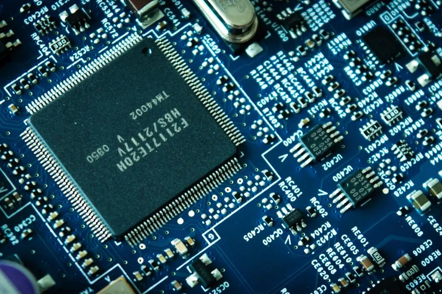
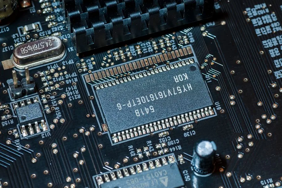
Introduction to Double Sided PCBs
If you’re creating anything more advanced than the simplest microcontroller circuit, you’ll likely want to upgrade from a single-sided to a double-sided PCB design.
As the name suggests, a double-sided PCB has conductive copper traces on both the top and bottom sides of the board. This opens up more possibilities for routing and optimizing the layout of your circuit.
With a single-sided board, you can place components and their connections only on one side. Anything complex will quickly become a tangled nest of traces and struggle to fit into the available space.
By upgrading to a double-sided PCB prototype, you instantly double the real estate for laying out your schematic. Traces can cross over each other, connectivity becomes more flexible, and you can achieve a cleaner, more efficient use of the board area.
This can significantly speed up iterations of your prototype. You won’t waste time puzzling about how to route connections in tight spaces or resort to less optimal workarounds. To simplify the design process, you can also avoid layer transitions and vias.
Double-sided boards offer more room for your creative PCB design ideas to flourish. The additional flexibility opens the doors to testing innovations faster and producing professional-grade prototypes.
For anything beyond basic circuits like LED blinkers or Arduino shields, double-sided PCBs are recommended as the best practice nowadays. The extra designing options will likely prove worth the modest increase in prototyping costs over single-sided boards.
Related Reading: Double Layer PCB: All You Need To Know About These Specially Printed Circuit Boards

Advantages of Double Sided PCB Prototyping
Using a double-sided PCB prototype offers several advantages that can significantly speed up the PCB development process.
- Simplify Layouts
A key benefit of double-sided prototypes is the ability to simplify the board layout. With only two layers, the layout can be less complex than a multilayer board, with fewer components and routing constraints. This simplicity speeds up the design process. - Increase Routing Space
With two sides, double-sided PCBs provide more space for traces and routing. This reduces congestion and makes it easier to route connections cleanly. The extra routing area enables a faster layout compared to single-sided boards. - Test in Parallel
Another major advantage is the ability to test the double-sided prototype in parallel with designing the final multilayer PCB. Engineers can verify component placement and routing while the multilayer board is still being designed. This saves significant development time. - Facilitate Design Iteration
Prototypes also facilitate rapid design iteration. Engineers can test different layouts, component placements, and routing approaches quickly. Issues can be identified and tweaked faster with a prototype. This iterative process reduces re-spins and speeds development. - Utilize Design Automation
Lastly, double-sided prototypes allow leveraging PCB design automation tools for faster layout. Autorouters, design rule checks, and other features simplify prototyping. Together with the other advantages, design automation enabled by double-sided boards accelerates the development process.
Related Reading:
Applications of Double Sided PCB Prototyping
Double-sided PCB prototypes are useful in various stages of the design process for verifying and accelerating development. Some key applications include:
- Validating Circuit Concepts
In the early design stages, low-cost double-sided PCB prototypes can quickly validate circuit concepts and functionality. Engineers can test new ideas and approaches without investing significant time and cost into multilayer boards. - Testing Layouts and Form Factors
Double-sided PCB boards are also useful for testing PCB layouts and form factors. A prototype can quickly verify the mechanical characteristics before final tooling and fabrication. This helps finalize physical dimensions and board shape faster. - Early Firmware and Software Integration
Prototypes enable early integration of firmware and software development with the PCB hardware. Engineers can develop code and debug with prototype boards earlier, reducing the overall development timeline.
The low cost and fast turnaround of double-sided PCB prototypes make them ideal for various testing applications in the design cycle. Utilizing them effectively at the right stages accelerates the overall PCB development significantly.
Design Considerations When Using Double Sided PCBs
While the benefits are substantial, switching to a double-sided design does introduce some important considerations to factor in:
- Component Placement
You need to determine the optimal placement of components on each side of the board. Balance is crucial – heavily loading one side can complicate routing and fabrication. Plan placement to minimize crossovers. - Via Design
Vias allow connections between layers but introduce cost and fabrication factors. Minimize vias through careful planning. Follow all design rules for via sizes, spacing, and plating. - Trace Routing
With more freedom comes more complexity in routing. Ensure traces don’t overload one side and keep high-speed signals isolated. Verify trace width and clearance rules are followed. - Thermal Management
With components on both sides, heat dissipation needs more consideration. Ensure adequate copper fills for heat sinks and air flow on each side. - Testing and Rework
Double-sided boards make probing and modifying circuits more difficult. Plan test points carefully and consider access needs for rework.
These are key factors to be aware of. With some experience, you will learn tricks to effectively manage this added complexity. The benefits outweigh the tradeoffs in most cases for prototype designs.
When to Choose Double Sided PCBs
Given the pros and cons, when should you make the decision between single sided or double sided PCBs for your prototype? Here are some guidelines:
- For any design more complex than a basic microcontroller circuit, double sided is recommended as best practice. The extra routing flexibility will save you time.
- If your design is space constrained, double sided allows components and traces to be more tightly packed and optimized.
- For mixed signal designs combining analog and digital, double sided makes isolating signals easier.
- High speed designs with many data lines or precise timing constraints will benefit from the routing control double sided provides.
- Multi-layer boards are expensive, so double sided is an affordable option to add “virtual” layers when cost is critical.
- If you are prototyping a design to reduce layer counts for final production, double sided is a key strategy.
The modest increase in prototype cost is generally well worth it compared to the advantages. For professional-grade electronic products, double sided PCB design is standard.
Of course, talk to your PCB manufacturer if you need help deciding what’s best for your specific design requirements and budget. But in most cases, starting with a double sided prototype PCB will provide superior results.
Conclusion
To wrap up, double sided PCB prototypes offer significant benefits for the majority of electronic designs:
- Faster iteration by optimizing trace routing with more space
- Enabling more compact and complex circuit layouts
- Lower costs by potentially reducing layer counts
- Better high speed performance through isolated routing
- Simpler mixed signal layout by separating analog and digital
With some extra care taken in component placement, via design, and thermal considerations, the advantages far outweigh the small increase in fabrication costs over single sided boards.
For professional-grade products beyond simple microcontroller circuits, double sided PCB design is recommended as standard best practice nowadays. The additional flexibility and routing density achievable will accelerate your product development and allow for more innovations.
Ready to get started on your next double-sided PCB prototype? JHYPCB offers fast, affordable prototype fabrication and assembly for double-sided boards. Get in touch today to discuss your project and get a free quote.
We hope this overview has shown you the many scenarios where upgrading to double-sided will benefit your design process. Take advantage of the additional options early prototyping provides to build the product you’ve imagined sooner.


