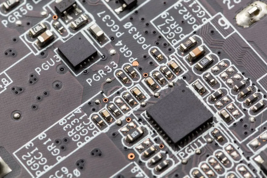
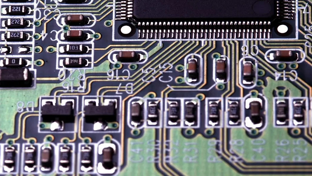
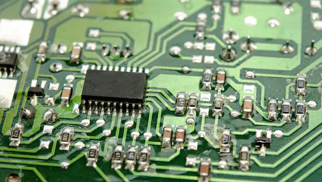
Double-sided printed circuit boards have become essential in many of today’s electronic devices and products. In contrast to their single-sided counterparts, which contain conductive traces on only one side, double-sided PCBs have conductive layers on both the top and bottom surfaces. This allows components to be mounted and connected on both sides of the board, enabling greater flexibility and optimization in the circuit layout.
Double-sided PCBs’ key advantage is increased component density within a given footprint area. Rather than only being able to place components on a single side, both sides of the board can be utilized in the design. This is critical for products where small size and weight are important factors, such as mobile consumer electronics, wearable devices, and medical equipment. It also helps reduce the overall dimensions of boards in larger products like telecom or server systems.
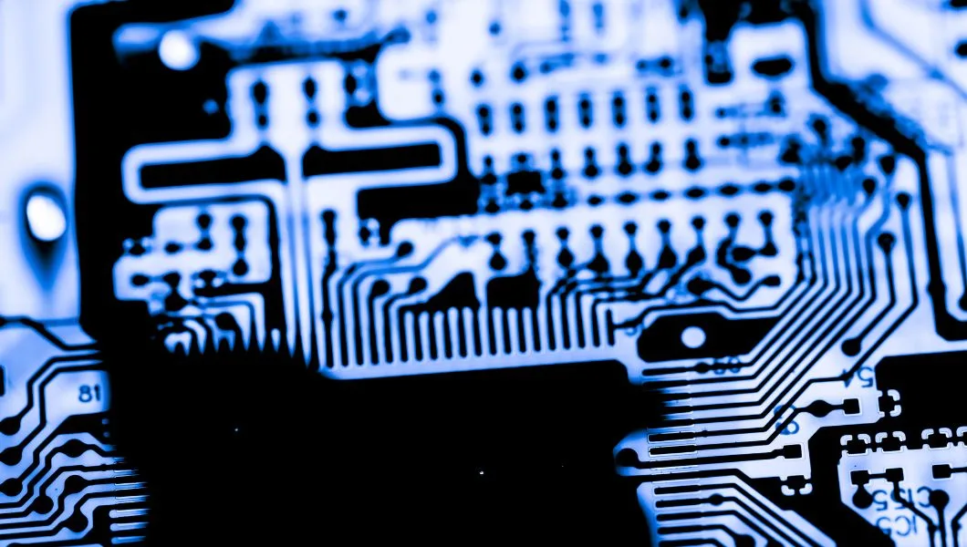
Double-sided PCB fabrication allows for more efficient routing of traces between components. With the ability to crossover traces between the top and bottom layers, designers have much more freedom in optimizing the layout to achieve compact designs and clean routing. This significantly improves key electrical parameters thanks to shorter trace lengths. It also often greatly simplifies the task of routing complex designs.
In summary, the expanded capabilities of double-sided PCBs have made them indispensable in various applications where functionality, reliability, and space utilization are key priorities. Their advantages over traditional single-sided boards have established them as a core technology enabling the compact, high-performance electronic products we use daily.
Applications of Double-Sided PCBs
Double-sided PCBs are utilized across a diverse range of industries and products to enable small, lightweight designs without compromising functionality or reliability.
- Consumer Electronics – Compact form factors and robust performance are critical for smartphones, tablets, and wearables. Double-sided PCBs allow complex circuitry and components to fit within extremely tight spaces. Apple’s Watch packs advanced sensory and processing capabilities into a chassis only 10mm thick thanks to its double-sided SMP PCB.
- Automotive – Engine control units (ECUs), infotainment systems, and ADAS components operate in harsh under-hood conditions while needing to process and transmit vast amounts of data. Double-sided PCBs enhance reliability and signal integrity in automotive environments while supporting complex, distributed electronic systems.
- Medical – Hearing aids, blood glucose monitors, and other health devices must balance compact size with reliable performance. Double-sided PCBs allow key medical devices to be minimally invasive and comfortable for users. Cochlear’s industry-leading hearing implants leverage double-sided PCB technology for their speech processors.
- Aerospace/Defense – State-of-the-art radars, navigation, and communications systems operate under extreme vibration, temperature, and g-forces. Rigorous testing ensures double-sided PCBs meet advanced defense platforms’ durability and performance needs.
- Telecom/Datacom – High-speed routers, servers, and network switches require maximum component density and signal integrity. Double-sided PCBs are essential for today’s high-bandwidth infrastructure, supporting 25Gbps designs and beyond.
This covers some of the key high-value applications where double-sided PCB technology provides differentiating capabilities and enables exceptional products. Their unique advantages and continual improvements will open the door to even more innovative applications.

Advantages Over Single Sided PCBs
Double-sided PCBs provide significant benefits compared to traditional single-sided boards thanks to their expanded capabilities:
- Increased Component Density – With components mounted on both sides, double-sided PCBs can accommodate more chips, passives, connectors, and other parts in a given footprint. This facilitates miniaturization and compact system designs.
- Better Trace Routing – Traces can crossover between layers through plated through holes, enabling shorter connections between components. This improves signal integrity and allows for complex routing schemes.
- More Complex Circuits – The added real estate and flexible routing enable more advanced circuit designs with higher component counts and capabilities. High-speed data paths also benefit.
- Improved Electrical Performance – With shorter trace lengths and better component placement and routing, double-sided PCBs offer lower inductance and other improved electrical parameters.
- Smaller Footprint – By utilizing both sides efficiently, double-sided PCBs can pack the same functionality into a smaller space than single-sided boards.
Other benefits include cost savings through smaller boards, simplified assembly, and reduced wiring harnesses. Continued PCB fabrication advances allow for finer lines/spaces, high layer counts, HDI, and other innovations to further leverage double-sided boards. Double-sided PCB technology is often the optimal choice for demanding applications over single-sided.
Related Reading: How To Tell single layer PCB From double-sided PCB?
Conclusion
Double-sided printed circuit boards have become indispensable across various industries and applications where small size, high reliability, and electrical performance are critical factors. They enable levels of miniaturization and functionality not practically achievable with single-sided PCBs.
Double-sided PCBs provide the ideal platform for complex, high-density electronics, from the latest consumer tech gadgets to mission-critical aerospace systems. Their ability to accommodate components and routing on both sides allows for optimization not possible with single-sided boards.
Continued innovations in PCB materials, fabrication techniques, and design tools will enable double-sided boards to push the envelope even further. 5G communications, autonomous vehicles, IoT devices, and other emerging technologies will rely on advanced double-sided PCBs at their core.
For electronic product developers, leveraging double-sided PCB technology provides tangible product size, performance, and reliability advantages. As PCB manufacturers like JHYPCB, we have extensive experience producing high-quality double-sided boards tailored for diverse applications. Please get in touch with us to learn more about how double-sided PCBs can benefit your next product design.
Related Reading