Introduction
With the ongoing miniaturization and increasing complexity of modern electronics, PCB designs must deliver higher functionality within compact spaces. This has driven demand for multilayer PCB configurations that allow greater routing density and component placement. The 8-layer PCB stackup has emerged as an optimal solution, providing the signal integrity, power delivery, and electromagnetic shielding needed for today’s dense circuits.
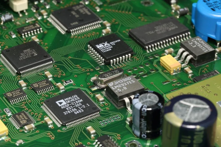
An 8-layer PCB refers to a printed circuit board composed of 8 conductive copper layers interleaved with insulating dielectric materials. The key benefits of the 8-layer stackup compared to lower-layer boards include the following:
- Enhanced signal integrity due to multiple ground and power planes
- Improved power distribution with dedicated power layers
- Reduced EMI through shielding planes between signals
- More routing channels to accommodate high component density
- Overall, better electrical and RF performance
While more complex than 2-layer or 4-layer boards, the 8-layer stackup offers an ideal balance of capabilities and cost-effectiveness. This makes it a popular choice for many high-density and performance-driven applications.
This guide will explore the key considerations for designing 8-layer PCBs, typical stackup configurations, materials used, best practices, and more. We’ll also examine the advantages of working with a specialized PCB manufacturer for your 8-layer boards. Let’s get started!
Key Considerations for 8 Layer PCB Design
When moving from a simpler 2 or 4-layer board to an 8-layer stackup, designers must account for several important factors:
- Signal Integrity
With higher speeds and greater interconnect density, maintaining signal integrity is crucial. The multiple ground planes in an 8-layer PCB helps control impedance and reduce cross-talk. However, controlled routing, layer separation, and termination are still required. - Power Distribution
The additional layers in an 8-layer board allow dedicated power planes to distribute current evenly across the PCB. Separating analog and digital power helps avoid noise coupling. Designers must size power planes appropriately and use enough vias/decoupling caps. - Electromagnetic Interference
Increased operating frequencies make EMI a significant concern. The shielding planes in an 8-layer stackup contain EMI within the board. A solid ground plane foundation and proper component placement and enclosure shielding are key. - Component Density
Adding more layers multiplies routing channels, allowing higher component densities. But, designers must ensure adequate clearance between parts and heat dissipation for thermally sensitive components. Careful floorplanning helps maximize the utilization of the 8 layers. - Cost
While more affordable than flex PCBs or exotic materials, 8-layer boards cost more than 2 or 4-layer configurations. Designers should evaluate whether the increased performance justifies the incremental cost. Simplifying layer stackup helps reduce costs.
Getting these elements right ensures an 8-layer PCB that meets circuit speed, density, noise, thermal, and budgetary requirements. We’ll highlight specific stackup arrangements and design practices to optimize your 8-layer board.
Typical 8 Layer PCB Stackup Configurations
There are several common arrangements of the 8 layers in a PCB stackup, each optimized for specific design goals:
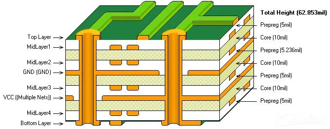
Standard Stackup
——————- L1 (Copper, Top Layer)
— Prepreg 1 —
——————- L2 (Routing, Signal Layer1)
— Prepreg 2 —
——————- L3 (Routing, Ground Plane 1)
— Prepreg 3 —
——————- L4 (Core, Signal Layer 2)
— Prepreg 4 —
——————- L5 (Core, Power Plane 1)
— Prepreg 5 —
——————- L6 (Routing, Signal Layer 3)
— Prepreg 6 —
——————- L7 (Routing, Ground Plane 2)
— Prepreg 7 —
——————- L8 (Copper, Bottom Layer)
This provides a robust stackup with good SI and EMI control. The middle ground plane isolates the two signal layers.
High-Speed Signal Stackup
——————- L1 (Top Layer)
— Prepreg 1 —
——————- L2 (Signal Layer 1)
— Prepreg 2 —
——————- L3 (Ground Plane 1)
— Prepreg 3 —
——————- L4 (Signal Layer 2)
— Prepreg 4 —
——————- L5 (Power Plane 1)
— Prepreg 5 —
——————- L6 (Signal Layer 3)
— Prepreg 6 —
——————- L7 (Ground Plane 2)
— Prepreg 7 —
——————- L8 (Bottom Layer)
With ground planes above and below the signal layers, this stackup is ideal for high-speed signals up to multi-Gbps speeds.
Mixed Signal Stackup
——————- L1 (Top Layer (Analog Signals))
— Prepreg 1 —
——————- L2 (Signal Layer 1 (Analog))
— Prepreg 2 —
——————- L3 (Ground Plane 1)
— Prepreg 3 —
——————- L4 (Signal Layer 2 (Digital))
— Prepreg 4 —
——————- L5 (Power Plane 1)
— Prepreg 5 —
——————- L6 (Signal Layer 3 (Digital))
— Prepreg 6 —
——————- L7 (Ground Plane 2)
— Prepreg 7 —
——————- L8 (Bottom Layer)
Separating analog and digital signals prevents noise coupling and interference.
Power Integrity Stackup
——————- L1 (Top Layer)
— Prepreg 1 —
——————- L2 (Signal Layer 1)
— Prepreg 2 —
——————- L3 (Power Plane 1)
— Prepreg 3 —
——————- L4 (Ground Plane)
— Prepreg 4 —
——————- L5 (Signal Layer 2 (Power Integrity))
— Prepreg 5 —
——————- L6 (Power Plane 2)
— Prepreg 6 —
——————- L7 (Signal Layer 3)
— Prepreg 7 —
——————- L8 (Bottom Layer)
The middle ground plane and focus on power integrity prevents voltage drops.
These examples illustrate how an 8-layer PCB stackup can be optimized for different design scenarios. We’ll cover more such arrangements and considerations further in the guide.
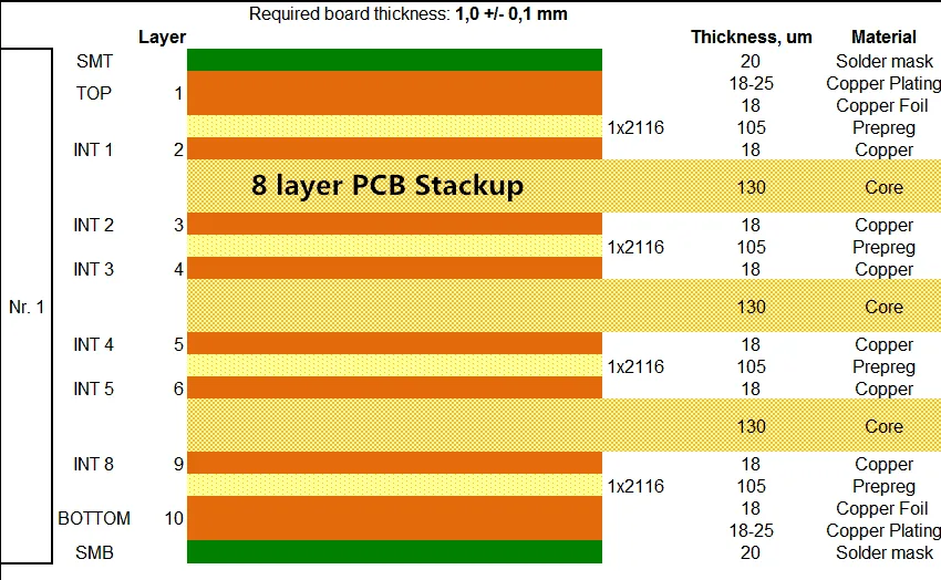
More 8 Layer PCB Stack-up Example
8 Layer PCB Stackup Materials
The conductive and dielectric materials used in an 8-layer PCB stackup are key in determining the board’s electrical, thermal, and mechanical characteristics.
- Conductive Layers
The conductive layers are typically made of copper foil, though other metals like aluminum or silver can also be used. Some key considerations for conductive layers include:
- Copper thickness – Standard 1/2 oz or 1 oz copper; thicker 2 oz copper used for high current
- Foil type – Standard electrodeposited or rolled copper; annealed copper is better for flex PCBs
- Surface finish – HASL, immersion silver, ENIG, OSP, etc.
- Dielectric Layers
The dielectric layers separate the copper layers, providing electrical isolation. Common dielectric materials include:
- FR-4 – Glass-reinforced epoxy; cost-effective, suitable for mainstream applications
- High-frequency/low-loss materials – PTFE, ceramic-filled PTFE, hydrocarbon ceramics; used for RF/high-speed boards
- High thermal conductivity – Alumina, aluminum nitride; for thermal management
Prepregs bond the copper and dielectric layers. Typical prepreg materials include FR-4, polyimide, and others.
The core layer in the center of the stackup requires a rigid, stable dielectric like FR-4 or polyimide. In some cases, metal cores are also used for thermal dissipation.
Understanding the properties and selecting appropriate materials is key to achieving target electrical, thermal, and mechanical objectives with the 8-layer PCB stackup.
Best Practices for 8 Layer PCB Stackup
While an 8-layer configuration provides more capabilities, designers must follow sound design practices to utilize it effectively:
- Impedance Control
Match trace widths and clearances to achieve target impedance based on stackup materials. Minimize length differences between related traces. - Layer Separation
Separate signals with similar functions on different layers. Interleave layers carrying high-speed signals with ground/power planes. - Signal Shielding
Route noisy traces over a ground plane and sensitive traces under a ground plane for shielding. Use guard traces around critical signals. - Ground Planes
Use a solid, unbroken ground plane whenever possible. Connect all grounds to the plane using thermal reliefs. - Balanced Layer Distribution
Distribute power and ground planes evenly through the stackup. Balance layer order and populate evenly to avoid warpage.
In addition, maintain a minimum clearance between traces and planes, establish robust power domains, enable thermal vias for heat dissipation, and simulate performance before layout.
Adhering to these guidelines helps avoid cross-talk, EMI, ground bounce, and impedance discontinuities. A well-designed 8-layer stackup delivers superior electrical, thermal, and mechanical performance.
8 Layer PCB Thickness and Dimensions
The thickness and dimensions of an 8-layer PCB depend on the materials used and design constraints. Some key considerations include:
Thickness
– Typical thickness is between 1.6mm to 3mm
– More layers make the board thicker to accommodate additional copper and prepreg
– Thicker copper and more prepreg/core layers increase the thickness
– Thinner materials can be used to reduce thickness where compactness is critical
Panel Size
– Standard PCB panel sizes include 12”x18”, 18”x24”, and 21”x24”
– Larger panel sizes are more cost-effective but limit board dimensions
– Individual PCB units can be cut from the panelized design
Aspect Ratio
– Length-to-width ratio from 1:1 up to 4:1 or more
– Higher aspect ratios allow longer board dimensions
– Aspect ratio impacts mechanical stability; thicker boards can accommodate greater ratios
Yearly layer count trends show increasing use of 8-layer boards as density and high-speed signal needs grow. Understanding PCB thickness constraints and standard panel sizes helps optimize manufacturability.
Benefits of Working with a Quality PCB Manufacturer
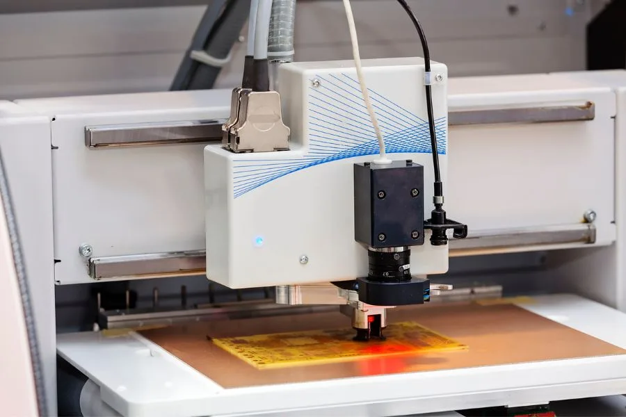
While 8-layer PCBs provide expanded capabilities, they present fabrication and assembly challenges that require an experienced manufacturer. Key benefits of working with a high-quality supplier like JHYPCB include:
- Expertise with Complex Boards
With over 15 years of experience, JHYPCB specializes in manufacturing complex multilayer PCBs, including 8-layer designs. Our engineers are highly trained to handle the lamination via formation, impedance control, and material handling needed for premium 8-layer boards.
JHYPCB utilizes advanced PCB production lines featuring the latest equipment for precise alignment, high-yield lamination, direct imaging, and other processes vital for quality 8-layer stackups. We continue to invest in facilities to meet the growing demand.
Every PCB produced undergoes rigorous quality assurance, including automated optical inspection, electrical testing, and X-ray inspection when required. This level of quality control is essential to reliably producing defect-free 8-layer boards.
- Customer Support
JHYPCB’s sales and engineering team can provide expert guidance on 8-layer stackup design considerations, material selection, DFM practices, and other aspects unique to your board. We help customers optimize their 8-layer PCB designs.
By leveraging JHYPCB’s proven 8-layer PCB capabilities, customers benefit from optimized stack-ups, rapid turnaround, and the highest quality boards.
Conclusion
As circuit densities and performance requirements continue to increase, the 8-layer PCB stackup provides an optimal solution. The additional routing layers, dedicated power/ground planes, and shielding capabilities enable complex, high-speed designs in a cost-effective package.
Key considerations covered in this guide include maintaining signal integrity, distributing power, minimizing EMI, accommodating component density, and controlling costs. We reviewed standard stackup arrangements like high-speed signal, mixed signal, power integrity designs, materials, and best practices.
While presenting fabrication challenges, partnering with an experienced PCB manufacturer like JHYPCB allows you to reap the benefits of 8-layer boards. Our expertise in multilayer PCBs, advanced production facilities, rigorous quality control, and engineering support enables us to deliver high-performing, reliable 8-layer PCBs tailored to your requirements.
With sound design principles and the right PCB partner, an 8-layer stackup unlocks the next level of electronics innovation for your product. Reach out to explore how we can optimize and efficiently manufacture your 8-layer PCB design.
Related Reading