


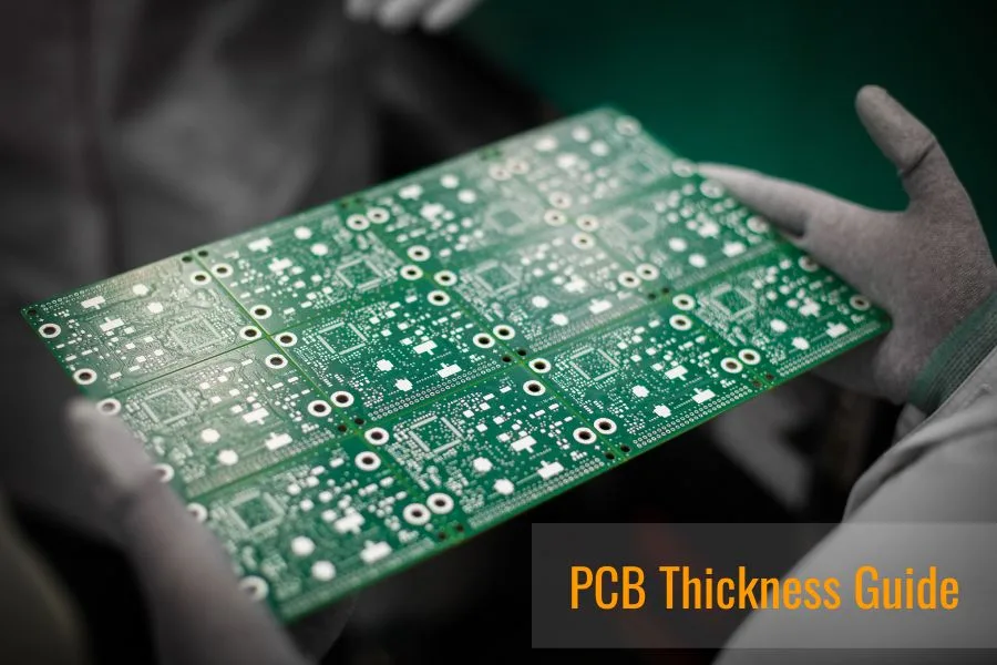
Your Trusted Prototype PCB Manufacturing And Assembly Partner.
When you partner with us, we do everything to ensure your PCB manufacturing and assembly are completed on time to your specifications with the highest quality.
Leading manufacturer of PCB Fabrication and Assembly in China.
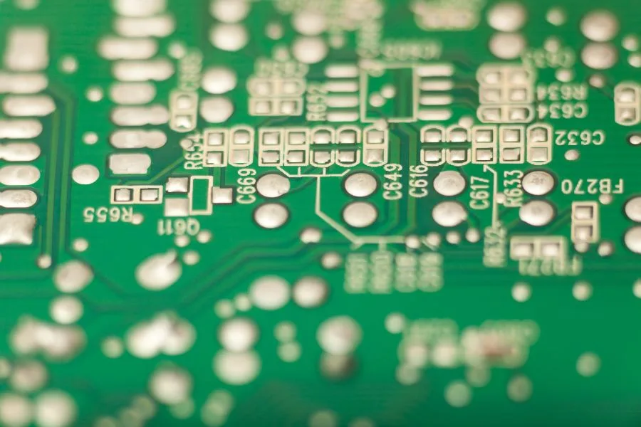
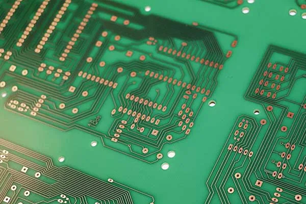
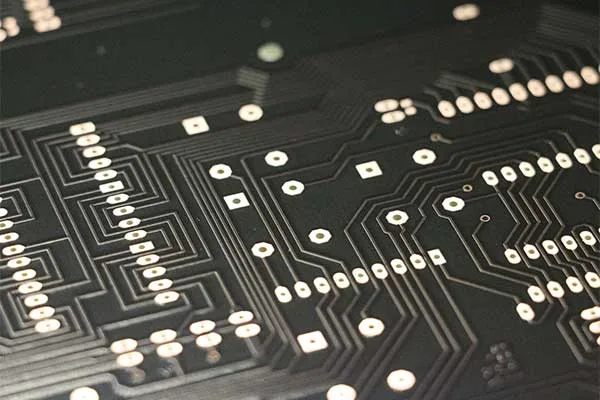
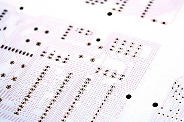
As a key component in PCB fabrication, the solder mask provides crucial protection and insulation for intricate copper traces. This thin layer, typically 30-60 microns thick, coats the entire PCB surface except for areas requiring soldering. While often overlooked, properly selecting and applying the solder mask material is critical for reliable PCB performance. The material properties like adhesion, chemical resistance, thermal stability, and dielectric strength allow the solder mask to endure soldering, cleaning, and operation in harsh environments. In addition to safeguarding PCB traces, the solder mask layer improves aesthetics and prevents solder bridging. This article will explore the various solder mask materials, critical solder mask properties, the application process, and key design considerations for utilizing solder masks effectively on your next PCB project.
A solder mask layer refers to the protective layer of polymer that coats the copper traces on the surface of a PCB. This thin coating is usually between 30-60 microns thick.
The key functions of the solder mask are:
A polymer layer is applied over the metal traces on a printed circuit board to create a solder stop mask. Depending on the cost and required application, different types of PCB solder masks can be used. A simple option is to use a silkscreen to print a liquid epoxy over the conductors, similar to airbrushing paint through a stencil. The solder mask is available in a wide range of colors.
There are four types of solder masks used in PCB fabrication:
The most widely used solder mask material is liquid photoimageable solder mask (LPSM). As the name suggests, LPSMs consist of a liquid coating that is photosensitive. The liquid mask is applied to the PCB surface by screen printing, curtain coating, or spray coating. Once applied, the mask is exposed to UV light through a patterned film. The UV light causes chemical changes in the exposed areas of the mask, which are then developed away to create openings in the mask layer.
LPSMs are typically epoxy-based materials that cure to form a robust polymeric coating when thermally treated after developing. Some advantages are excellent chemical resistance, adhesion to the PCB substrate, and thermal stability to withstand soldering temperatures.
Popular examples of LPSMs include Taiyo PSR-4000 series, Coates Vialux, and DuPont Vacrel.
Dry film solder mask consists of a photosensitive layer laminated onto the PCB as a solid sheet, rather than a liquid. The dry film is vacuum applied over the board and requires heat and pressure to adhere it to the PCB surface. Like LPSM, the dry film is then exposed to UV light through a pattern and developed to create openings.
Dry film masks have some advantages in ease of handling and application speed. However, they tend to be more expensive than liquid masks and have some drawbacks in resolution capability.
The most common type of solder mask for PCBs is utilizing a silkscreen to apply a liquid epoxy onto the surface. This is a cost-effective and widely used option for solder stop masks. The process involves using a mesh screen to create ink-blocking patterns on the PCB. The liquid epoxy utilized is a thermosetting polymer that will harden when subjected to a thermal cure process. The desired color of the solder stop mask is achieved by mixing the solder mask dye into the liquid epoxy and allowing it to cure.
In other guides discussing PCB solder mask types, you may come across the terms “top-side” and “bottom-side” masks. These terms simply refer to the specific location of the solder mask on the PCB, and do not necessarily indicate a certain type of manufacturing process or material used for the solder mask. It is important to include a solder mask on the top side of a board as this allows for easier access to the holes and pins for electronic engineers. The solder mask is typically applied using film, ink, or epoxy methods. The copper traces on the upper side of the board are referred to as “top traces,” while those on the lower side of the board refer to the connections made through the holes.
The properties of the solder mask material determine how well it can provide the necessary protection and withstand the PCB fabrication process and operating conditions. Some key properties include:
Carefully evaluating solder mask needs across these properties ensures finding the right material for the application. The material formulation impacts properties like flexibility vs. hardness. Finding the optimal balance is key.
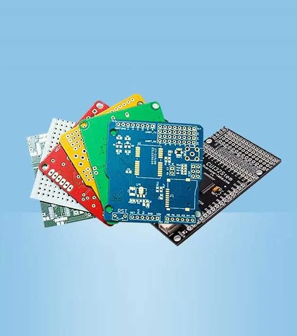
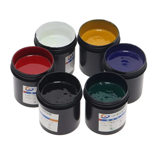
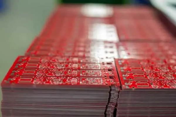
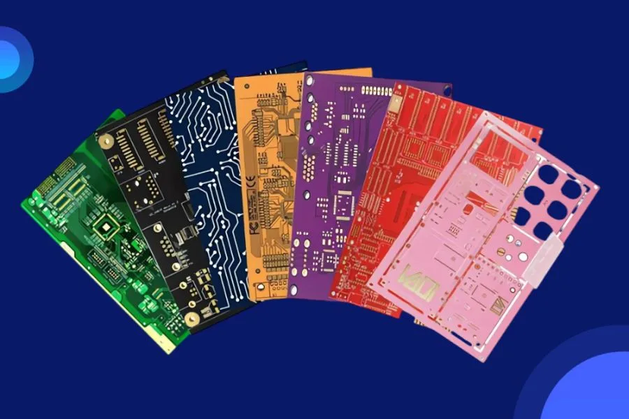
There are now many more options to choose from when it comes to PCB solder masks than the traditional green finish. These masks are now available in a variety of different colors, both glossy and matte. By selecting different colors, you can easily differentiate between your various printed circuit boards and match them to your personal preferences.
If you’re looking for a wider selection of colors, glossy finishes are the way to go. These finishes offer a broader range of color options, including green, black, red, yellow, white, purple, and blue. However, if you prefer a matte finish, your options are more limited. Currently, only green and black colors are available in a matte finish.
While there is no clear reason why green is the most popular color for solder masks, it might be because it creates the smallest solder dam (space) compared to other available colors.
In addition, green has been proven to be the most visible color to the human eye in daylight, making it easier to work on and use PCBs with green solder masks. This color is also easily recognizable and makes it simple to locate PCBs with green masks, further contributing to its popularity.
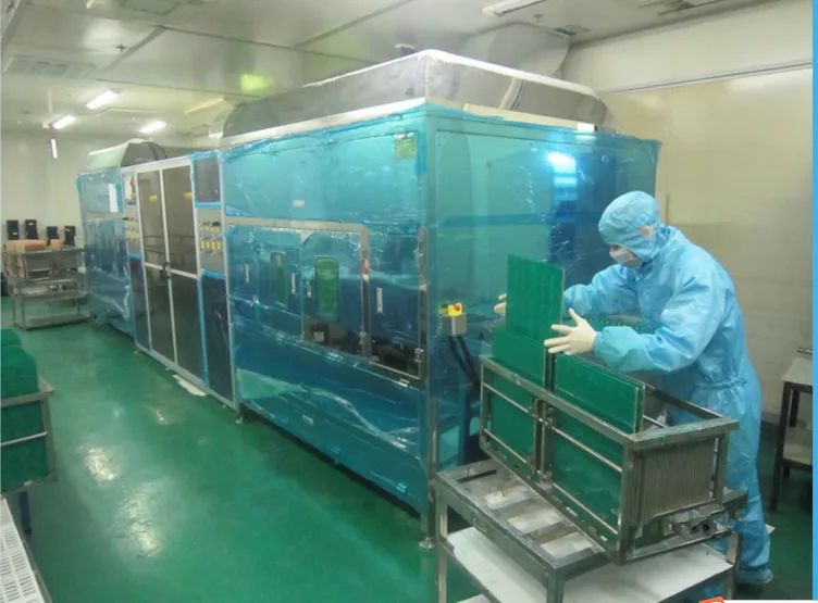
The process of applying a solder mask involves several essential steps. These include:
Pre-treatment:
This step involves treating the copper layer by preheating to prevent oxidation and make it more adhesive.
Coating:
After pre-treatment, the solder mask is applied to the PCB board using screen printing. The color of the mask is based on the customer’s requirements.
Drying:
The PCB board is then left to dry for about 15 minutes before pre-baking. This assists in minimizing solvent evaporation during pre-baking.
Pre-baking:
The process of pre-baking continues the evaporation of solvent ink in the tunnel oven. Temperature, ventilation management, and time control are important aspects to consider.
Registration:
Registration is done with the help of the film after pre-baking.
Exposure:
The glass frame and polyester film are checked before switching on the vacuum area and selecting an exposure program.
Developing:
This step involves getting rid of the solder solvent that may still be present on the pads in shading sections. Sodium carbonate is used in a 1% concentration, and the temperature of the liquid should be maintained at 28-32 degrees Celsius.
Inspection:
An inspection is required to remove any burrs or defect images.
Final curing:
This last step involves placing the PCB board in the tunnel oven for baking and thermal curing. Sometimes, UV curing can be used to improve the mechanical and chemical characteristics of the solder stop.
The solder mask layer impacts PCB design and layout in several key ways:
In summary, the solder mask footprint design affects manufacturability, soldering yield, and reliability. Optimizing the mask layout requires balancing factors like bridge prevention and component anchoring.
The solder mask thickness will depend primarily on the thickness of the copper traces on the printed circuit board. Typically, the solder mask thickness is at least 0.8 mils perpendicular to the board, but it can vary based on the location. Near the edges of traces, the solder mask can be thinner, sometimes as thin as 0.3 mils or less. In general, it is recommended to have about 0.5 mils of solder mask over traces.
The solder mask serves not only to prevent corrosion on copper traces but also to place a dam between neighboring pads on a circuit board. For component pads, a small gap is defined between the solder mask and exposed pads, called a solder mask relief. This creates a dam that prevents molten solder on one pad from flowing onto a neighboring pad. This is especially important in fine-pitch BGAs and other high-density components. The small relief around the edge of a pad allows the droplet of solder to wet the pad and hold itself in place, which helps prevent bridging during soldering. Sprayed epoxy solder mask is an option that can provide a more uniform thickness throughout PCB.
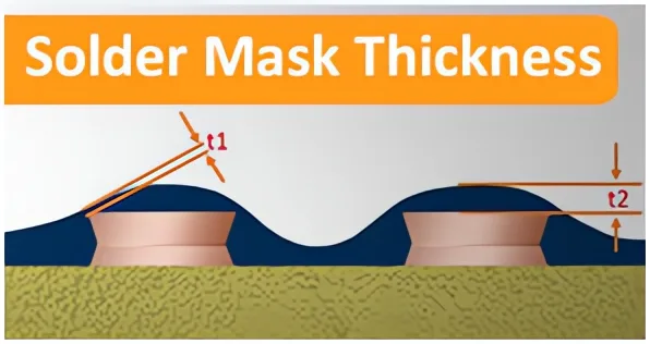
PCB Solder Mask Thickness:
Employing a solder mask during PCB fabrication and assembly provides several important benefits:
Solder masks and paste masks are two different but related things used in the manufacturing of PCBs.
A solder mask is a type of coating that is applied to the surface of a PCB to protect it from oxidation and prevent solder bridges between conductive areas during the assembly process. It is typically green in color and is applied to the entire surface of the PCB, leaving only the metal pads and through-holes exposed. This allows the solder to be applied only where it is needed.
On the other hand, a paste mask is a type of stencil that is used to apply solder paste to the surface of the PCB during the assembly process. It is typically made of a thin sheet of material with openings cut out to match the location of the metal pads on the PCB. When the paste is applied to the stencil and scraped across its surface, the paste is deposited onto the PCB only where the openings are located.
Key Differences:
In the context of PCB manufacturing, Solder mask, and Solder resist are essentially the same thing. They are both used to protect the surface of the PCB and prevent short circuits during assembly. Both solder mask and solder resist are applied to the surface of the PCB after the copper traces have been etched and before the components are mounted.
However, the two terms are often used interchangeably in different regions and industries. Solder mask is more commonly used in North America and Europe, while solder resist is more commonly used in Asia. Additionally, some manufacturers may use one term instead of the other to emphasize specific features, such as flexibility, thermal resistance, or UV resistance.
Solder mask is a thin layer of coating applied to the surface of a PCB to protect the copper traces and prevent short circuits during assembly. It also helps to prevent oxidation and surface contamination.
Solder mask is typically made from a liquid epoxy or liquid photoimageable (LPI) ink that is cured into a solid polymer upon exposure to heat or UV light.
Green is the most common color used for solder mask because it provides a good contrast to the copper traces and components on the PCB. However, other colors such as red, blue, black, and white are also available.
Solder mask is typically applied to the PCB using a process called screen printing, where a stencil is used to apply the solder mask to the surface of the board. It can also be applied using a dry film or liquid photoimageable (LPI) process.
Yes, solder mask can be removed using a chemical stripping process if it gets damaged or needs to be repaired. However, the process can be time-consuming and may require specialized equipment.
The thickness of the solder mask layer depends on the specific application and the requirements of the manufacturer. However, a typical thickness range for solder mask is 0.05mm to 0.10mm (2-4 mils).
It is not necessary to apply solder mask to both sides of a PCB, but it can provide additional protection and improve the overall appearance of the board.
The solder mask layer is typically non-conductive and should not affect the electrical performance of the PCB. However, excessive thickness or buildup can affect the thermal and mechanical properties of the board.
Yes, all solder masks are RoHS compliant.
Peelable solder mask, also known as peelable mask, is a temporary solder mask used in the PCB manufacturing process. It is typically applied after the normal permanent solder mask has been applied, allowing the PCB to be selectively soldered. The peelable mask can then be peeled off to reveal the copper pads for soldering and then re-applied if required. Its main purpose is to protect the areas of the board that are not intended to be soldered, such as the gold fingers or edge connectors. Peelable solder masks are typically made of a synthetic rubber material that can be easily removed by hand or with a simple tool.
In a typical wave soldering process, the solder mask is designed to endure high temperatures of molten solder for a short period, approximately one second. The majority of the commercially available solder masks possess the ability to withstand the melting point temperatures of both lead-based and lead-free solder, around 650°F (or 343°C).


When you partner with us, we do everything to ensure your PCB manufacturing and assembly are completed on time to your specifications with the highest quality.
Fill out the form below, and we will get back to you within the next 24
hours to complete the order, and then you’re all set to get started!