


Your Trusted Prototype PCB Manufacturing And Assembly Partner.
When you partner with us, we do everything to ensure your PCB manufacturing and assembly are completed on time to your specifications with the highest quality.
Leading manufacturer of PCB Fabrication and Assembly in China.
Whether you’re a designer, engineer, or PCB manufacturer, understanding the benefits and design considerations of Via-in-Pad is crucial for achieving efficient and reliable circuit board designs. In this article, we will explore the basics of Via-in-Pad, including its importance, advantages, different types, and design guidelines, as well as its manufacturing process, applications, and summary. By the end of this guide, you’ll have a better understanding of Via-in-Pad and how it can enhance your PCB designs.
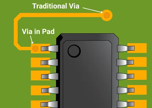
Via-in-Pad, also known as VIP or plated through-hole (PTH) technology, is a method of creating electrical connections between the different layers of a printed circuit board. A via is a hole drilled through a particular layer of the PCB, and Via-in-Pad refers to the process of plating the inner layer of the via, which allows an electrical connection to be made between the layers. Via-in-Pad technology is often used in high-density circuit applications and enables the designers to reduce the overall size of the PCB.
Via-in-Pad technology has become increasingly important in PCB manufacturing due to the growing trend towards miniaturization of electronic devices. With the increasing demand for smaller and more complex products, the traditional methods of connecting different layers of the PCB are no longer adequate. Via-in-Pad technology enables the designers to reduce the size of the PCB and increase the density of circuitry, whilst maintaining high levels of performance and reliability.
In addition to allowing for smaller and more complex designs, Via-in-Pad technology can also offer significant cost savings compared to traditional methods of connecting different layers of the PCB. By reducing the number of drilled holes on the PCB, the manufacturing process becomes more efficient, and the overall cost of production is lowered.
Overall, Via-in-Pad technology is an essential technique for modern PCB design and manufacturing. Its ability to enable smaller, lighter, and more reliable electronic devices makes Via-in-Pad a critical component of the electronics industry.
Via-in-Pad technology is becoming increasingly popular in PCB manufacturing due to its numerous advantages. Some of the key advantages of Via-in-Pad technology are:
Reduced dimensions: With traditional vias, you need to allocate extra space on the board for placing the via. However, with Via-in-Pad technology, the via is placed directly within the pad, which allows you to reduce the overall size of the board.
Increased density: Via-in-Pad technology allows for higher routing density on the board since the via is placed within the pad. This enables you to add more components or routing channels on the board.
Improved thermal management: Via-in-Pad technology helps to dissipate heat from the components and helps to keep the temperature of the PCB in check. This is particularly advantageous for high-power applications where thermal management is critical.
Increased design flexibility: With Via-in-Pad technology, you can place the via anywhere on the pad, allowing greater flexibility in the design of the PCB. This gives you the freedom to create more complicated designs and adds to the overall functionality of the device.
When it comes to Via-in-Pad, there are various types available. In this section, we will outline the most common types of Via-in-Pad:
Non-conductive Via Fill:
This type of Via-in-Pad involves filling the via with non-conductive material, typically epoxy, to ensure that the solder mask and copper plating will not flow into the via, thereby keeping it free from any short circuits. This is an economical option that is widely used in most PCB designs.
Copper Via Fill:
Copper Via Fill is a technique that involves filling the via with copper instead of non-conductive material. This option improves thermal conductivity and electrical performance, as well as provides additional structural reinforcement. It is more expensive than non-conductive via fill, but its enhanced properties make it an ideal choice for high-end PCB designs.
Silver Via Fill:
Silver Via Fill is a more expensive option that involves filling the via with silver, which is an excellent conductor of heat and electricity. This option has better thermal conductivity and is a good choice for PCB designs that require high-frequency signals or high thermal dissipation.
Gold Via Fill:
Gold Via Fill involves filling the via with gold, which provides superior electrical conductivity and effectively prevents oxidation. The gold plating is costlier than copper and silver, but the added benefits of corrosion resistance and excellent conductivity makes it an excellent choice for mission-critical PCB designs.
In summary, the choice of Via-in-Pad type depends on the specific requirements of the PCB design, such as thermal management, electrical conductivity, and cost constraints. The four options outlined here are all widely used and deliver excellent results depending on the intended application.
Via-in-Pad technology has become increasingly popular in modern PCB design. When designing via-in-pad, it is important to consider the following factors:
Pad size: The pad size should be designed to suit the size of the via and the component pin size. Generally, the pad size should be slightly larger than the via size to ensure a good connection.
Hole size: The hole size of the via should be designed based on the diameter of the drill bits used in PCB production. It is recommended to add a small amount of tolerance to ensure that the via can be drilled accurately.
Annular ring size: The annular ring is the copper around the via hole. The size of the annular ring is important because it affects the electrical performance and reliability of the PCB. The size of the annular ring should be large enough to ensure a good connection, but not too large, otherwise it may cause solder short circuits.
Minimum spacing: The distance between the via and other conductors on the PCB should be considered to avoid electrical interference. The minimum spacing between the via and other traces depends on the design rules specified by the manufacturer.
Plated vs non-plated vias: Plated vias are commonly used in PCB design because they provide better electrical connection and reliability. Non-plated vias may be used in certain situations, such as for test points, but they are generally not recommended for critical applications.
Initially, the PCB designer incorporates Via-in-Pad technology into the PCB layout. During the manufacturing process, the PCB vendor drills holes (Vias) through the PCB’s outer copper layer at the locations where Vias are required. The next step is to create a Via tenting layer, a process in which a layer of insulating material is applied to seal the via hole.
Following this, the PCB is coated with a layer of photosensitive resist, which is selectively exposed and developed to reveal the PCB’s required copper traces and pads. The manufacturer then uses electroplating to add layers of copper to the board. During the copper plating process, the holes (Vias) are also plated, forming a direct connection between different layers of the PCB.
Once the electroplating process is complete, the manufacturer removes the excess resist, exposing the copper traces and pads. The PCB is then cleaned to remove all remaining residues.
The final step is to apply a solder mask that protects the copper traces and pads of the PCB. The mask is selectively applied to prevent coverage of the Via holes, ensuring a clear opening for the Via’s connection points.
The Via-in-Pad creation process during PCB manufacturing requires accurate drilling, electroplating, and solder mask application to produce a PCB that functions accurately. Careful consideration of elements such as Pad size, hole size, annular width, minimum distance, and whether or not to copper plate holes plays a vital role in ensuring a reliable product.

Via-in-Pad technology has become an increasingly popular option in PCB design due to its various applications. In this section, we will discuss the different ways Via-in-Pad can be utilized in PCB designs.
Via-in-Pad technology can be used as an effective solution for thermal management in PCB designs. By placing copper-filled vias directly under SMD pads, heat dissipation from the component can be greatly improved. This is especially useful in applications where high power components and thermal management are critical, such as in LED lighting applications or power electronics.
Another application of Via-in-Pad technology is to improve signal integrity in high-speed PCB designs. By using blind or buried vias to connect inner layers to surface pads, signal pathways can be reduced, minimizing signal loss and cross-talk between traces. This is especially important in high-speed designs such as those found in communication systems or data centers.
Via-in-Pad technology can also increase manufacturing efficiency. By allowing vias to be placed directly under surface mount components, the total area required for the board can be reduced, ultimately reducing PCB size and thereby lowering costs.
Via-in-Pad technology is a critical element in high-density interconnect designs. With HDI designs, the aim is to pack as many components as possible on a smaller board. Via-in-Pad technology makes this possible by allowing more vias to be placed in smaller areas, allowing more routing freedom and greater component density on the board.
Via in pad is often used in PCB design to address various issues such as thermal management, signal integrity, and high density interconnect design. It is especially useful in designs where space is limited and the number of layers is restricted.
Via-in-pad is a PCB design technique that involves placing a via (metallic hole) within the pad of a PCB component, which improves thermal and electrical performance, and increases design complexity and cost.
The benefits of using via-in-pad include improved thermal dissipation, increased routing density, reduced signal coupling, and enhanced electrical performance.
The challenges associated with via-in-pad include difficulty in drilling and plating the via, increased manufacturing complexity and cost, and potential for pad lifting or circuit failures due to thermal-stress during reflow soldering.
Factors to consider when designing with via-in-pad include trace and via spacing, via placement and size, drill aspect ratio, copper plating thickness, and cost and manufacturability considerations.
Issues with via-in-pad can be avoided or minimized by carefully choosing the PCB manufacturer, using appropriate design rules and guidelines, following best practices for pad design and layout, and conducting thorough testing and validation of the final design.
Via in Pad can help to reduce the number of required layers by allowing for connections to be made between different layers through the via in pad, helping to save space and reduce costs.
When you partner with us, we do everything to ensure your PCB manufacturing and assembly are completed on time to your specifications with the highest quality.
Fill out the form below, and we will get back to you within the next 24
hours to complete the order, and then you’re all set to get started!