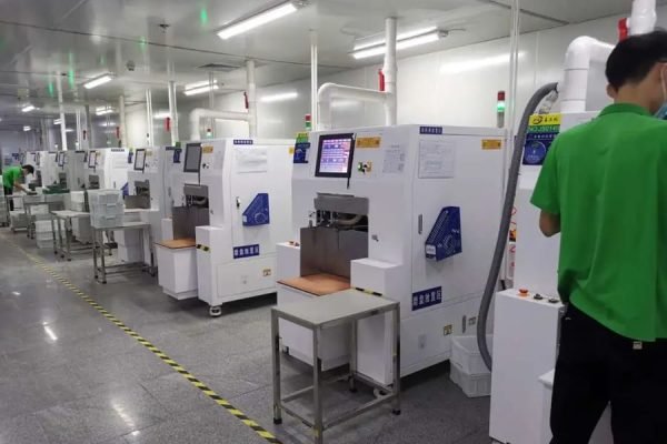
PCB Manufacturing Process
Plated Through Hole vs. Non-Plated Through Hole: A Comprehensive Comparison
The through-hole technology plays a crucial role in modern printed circuit board designs. These holes allow for connections between components and conductors on different layers of the board. Popularized during the construction of second-generation computers, through-hole technology can be either plated or non-plated. Both plated through-hole and non-plated through-hole refer to drilled holes on a circuit board, with slight differences in their manufacturing processes and applications.
PCBs are an essential component in modern electronics, enabling the devices we use every day to function. To create a PCB, a number of steps must be followed, including the etching of copper traces, the drilling of holes, and the insertion of components. One critical step in this process is the creation of holes that enable the connection of copper traces between different layers of the PCB. There are two primary types of holes used in PCB manufacturing: plated through holes (PTH) and non-plated through holes (NPTH).
Plated through holes involve the process of applying a layer of metal, typically copper, to the walls of the drilled hole. This process provides a solid connection between the different layers of the board and is commonly used in multilayer PCBs. The process of creating plated through holes requires several additional steps and can be more time-consuming and expensive than creating non-plated through holes.
Non-plated through holes, on the other hand, do not involve the application of a metal layer and are commonly used in single-layer and double-layer PCBs. The main advantage of NPTH is that they are easier and quicker to produce than PTH and also reduce the risk of electrical shorts and other manufacturing defects.
In this article, we will provide a comprehensive comparison between plated through holes and non-plated through holes in terms of their manufacturing process, advantages, disadvantages, and other key factors. We will also discuss the use of Via holes and multilayer PCBs, and provide recommendations for which type of hole to use based on the specific requirements of your project.
Overall, understanding the differences between PTH and NPTH is critical to the success of any PCB manufacturing project. By examining the benefits and drawbacks, we can make informed decisions on which type of hole to use in our designs. We hope this article will provide valuable insights and help you to make more informed choices in your PCB manufacturing process.
Table of Contents
Add a header to begin generating the table of contents
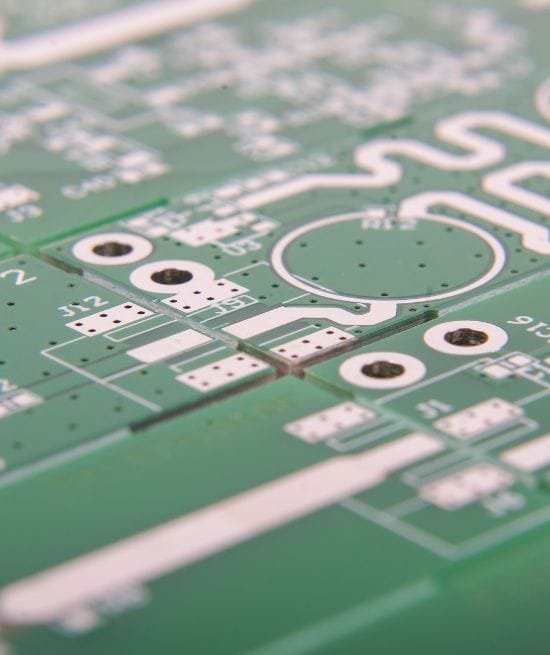
Via Holes in a Printed Circuit Board
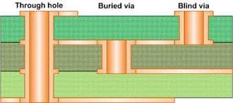
PCB via holes can be classified into three types: through holes, buried vias, and blind vias. Through holes are further categorized into two types: plated through-hole and non-plated through-hole. PTH vias are lined with a conductive material that allows for electrical connections to be made between layers of the board, while NPTH vias are not lined and are used only for mechanical support or to convey signals from one layer to another without electrical connection. Buried vias are completely contained within the layers of the PCB and do not extend to the board’s outer surface. Blind vias start from the outer surface of the PCB and extend to an inner layer but do not go through to the opposite side of the board.
What is Plated-Through Hole?
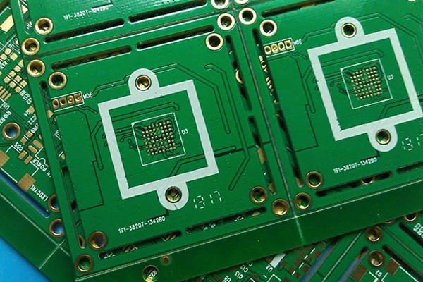
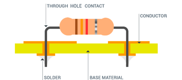
A Plated-through hole is a type of hole drilled in a printed circuit board that can be coated with a thin layer of metal to electrically connect the different layers of the board. The metal layer provides a reliable electrical connection between the different layers of the PCB. PTHs are commonly used in multilayer PCBs, which are used in more complex electronic devices.
Plated through holes Features
Plated through holes have several key characteristics that make them useful in PCB manufacturing:
- Conductive Functionality: PTHs are designed to provide a reliable electrical connection between the different layers of the PCB. They are coated with a thin layer of metal, usually copper, during the PCB manufacturing process to make them conductive.
- Inter-Layer Connection: Since PTHs can connect the different layers of the PCB, they are particularly useful in multilayer PCBs where there is a need to connect different layers of circuitry. Via holes are a specific type of PTH that allow the circuitry to be routed from one layer of the PCB to another.
- Currently, the majority of printed circuit boards are double-sided or multi-layered, and the majority of through holes are plated.
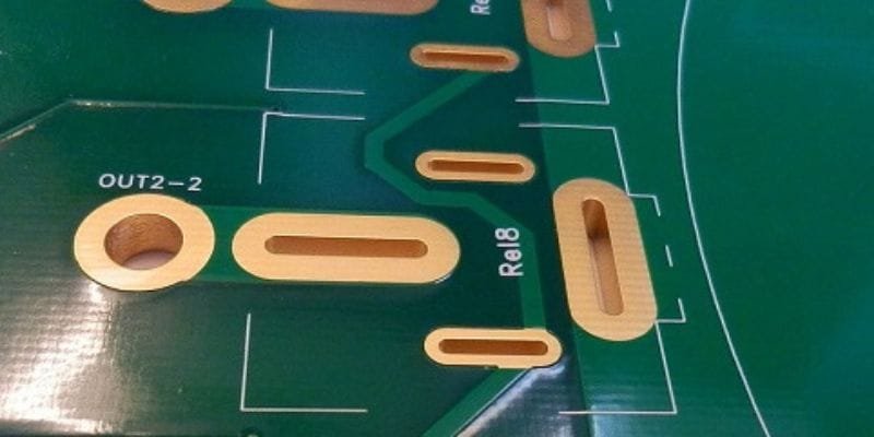
- Plated-through holes can take the form of plated slots or plated half-holes (also known as castellated holes), and they are not always round in shape.
Plated Through Hole Manufacturing Process
The manufacturing process for plated through holes typically involves three main steps: drilling, cleaning, and chemical copper plating.
Step 1. Drilling:
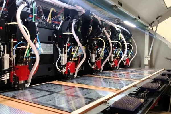
The first step is to drill a hole through the PCB substrate material. This is typically done by using a CNC drilling machine, which is capable of drilling thousands of precisely positioned holes into the substrate. The drilled holes are typically small, ranging in diameter from a few thousandths of an inch to a few hundredths of an inch.
Step 2. Cleaning:
After drilling, the PCB substrate is cleaned using a combination of chemical and mechanical processes. The goal of the cleaning process is to remove any debris or contaminants that may have been introduced during drilling, as well as any remaining substrate material that was not removed during the drilling process. The substrate is typically washed in a series of cleaning solutions, including degreasers, solvents, and acid baths, to ensure that it is entirely clean and free of any debris.
Step 3. Chemical Copper Plating:
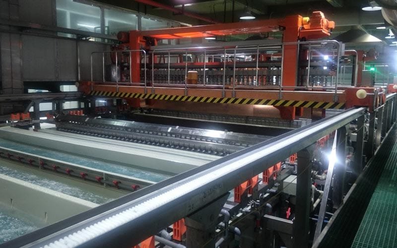
The final step in the manufacturing process for plated through holes is to chemically plate the copper onto the walls of the drilled holes. This is done by immersing the substrate in a chemical bath filled with a copper electroplating solution. The process of electroplating involves applying an electrical current to the substrate, which causes copper ions to be deposited onto the walls of the holes.
The result of this process is a plated through hole that is electrically conductive and mechanically strong. This allows the PCB to be used in a wide range of applications, including those that require high levels of electrical conductivity, such as those found in computers, mobile devices, and other electronic devices.
What are the challenges of plated through holes?
Plated through holes present several challenges in PCB design, and it’s important to consider these challenges and potential solutions. One major challenge is the lack of adequate copper in the PTH, which can cause plating voids that negatively affect current flow. Avoid too little or too much copper in the PTH to prevent this problem. Additionally, overly aggressive acceleration treatments can cause a lack of copper in the plated hole.
The proper construction of plughole is also crucial, as it prevents short circuits and flux residue from reaching the vias. If plugholes are not properly constructed, the entire PTH circuit board can be damaged. Failure to properly filter the system for copper particles can also cause copper to not liquidate well. Thus, it is essential to check the filtering system for any faults to prevent this from happening.
Lamination and blistering on a printed circuit board are also major concerns for PCB manufacturers. These problems can often be avoided by maintaining cleanliness and using an appropriate conformal coating. The combination of conformal coating and solder of the circuit board should help to achieve a good bond. Lamination on the circuit board due to oil stains and adhesives can be solved through pressing and drilling to remove these contaminants.
What is Non-plated Through Hole?
A non-plated through hole (NPTH) is a type of hole that goes through a PCB but does not have metal plating on the wall of the hole. In contrast, a plated through hole has metal plating on the wall of the hole, which provides electrical conductivity and mechanical stability. NPTHs are typically used for mounting components such as screws, standoffs, and connectors, or for providing a hole for testing points or jumpers that do not require electrical connectivity.
Non-plated Through Hole Features
- They do not have metal plating in their walls, which means they do not provide electrical conductivity or mechanical stability.
- They can be used for component placement or as test points, but they cannot be used for electrical connections between layers.
- They are typically drilled using lasers or mechanical drills, and then filled with an insulating material to prevent the flow of current.
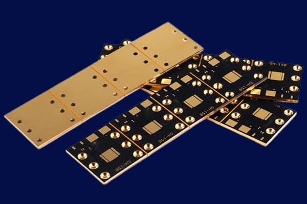
- They are often more expensive to manufacture than plated through holes because they require additional steps to fill and insulate the holes, , especially in aluminum PCB or copper base PCB.
- They are not suitable for high-density designs, as they take up more space on the PCB and cannot be used for interconnecting layers.
- They can be used for mounting components on the top or bottom layer of the PCB, or for providing clearance holes for mechanical hardware.
Non-Plated Through Hole Manufacturing Process
The NPTHs are different from PTHs in terms of both functionality and the manufacturing process. The NPTH manufacturing process involves several steps to fill and insulate the holes, making it more complex and expensive compared to PTHs. Let’s discuss the NPTH manufacturing process in detail.
First, the PCB is designed with NPTH locations specified.
Next, the PCB is drilled with either a laser or mechanical drill to create the non-plated through holes.
After drilling, the NPTHs are filled with an insulating material to prevent the flow of current. This could involve filling the holes with resin or plugging them with non-conductive materials.
Any excess insulating material is removed from the surface of the PCB, leaving the NPTHs filled with insulation.
The PCB is then cleaned to ensure that there is no residual material left on the surface or in the NPTHs.
PTH Vs. NPTH – What is the difference?
There are several challenges that can arise during the process of designing PCBs. One common issue is the potential difficulties posed by plated through holes and non-plated through holes. It’s important to understand the distinctions between these two types of through holes in order to create an effective circuit board. Familiarizing yourself with their unique functions and appropriate applications will help you to design a PCB that meets your needs.
| Feature | Plated Through Hole (PTH) | Non-plated Through Hole (NPTH) |
|---|---|---|
| Definition | A hole drilled into a PCB and then lined with a conductive material. | A hole drilled into a PCB and not lined with a conductive material. |
| Purpose | Conduct electrical current between different layers/sides of PCB. | Mechanical support/connection or as a capacitor or resistor. |
| Manufacturing | Requires an additional plating process | Easier to manufacture than PTH |
| Cost | Generally more expensive than NPTH | Generally less expensive than PTH |
| Design | Used when holes need to be plated for electrical conductivity | Not required for holes that don't need to be electrically conductive |
Through-Hole Vias Vs. Blind Vias - What is the difference?
| Criteria | Through-Hole Vias | Blind Vias |
|---|---|---|
| Conductive Function | Through-hole vias span the entire PCB thickness, providing electrical connectivity between all layers of the board. Their conductive function is highly reliable and consistent. | Blind vias only connect some of the layers of a PCB and do not span the entire board. Their conductive function is less stable than through-hole vias. |
| Application Scenarios | Through-hole vias are used when components need to be connected on both sides of the board or when there are more than two layers in a board. They can also be used in high-current or high-thermal applications. | Blind vias are used when space is limited, such as in small or thin devices. They are also used when certain layers of a board need to be isolated from others. |
| Manufacturing Costs | The cost of drilling through-hole vias is relatively low because they can be drilled after all the layers of a board have been laminated together. However, the cost of plating through-hole vias can be higher due to the additional copper plating required. | The cost of drilling blind vias is relatively high because each layer of a board needs to be drilled individually. However, the cost of plating blind vias is lower because they require less copper plating than through-hole vias. |
Through-hole technology in PCB assembly
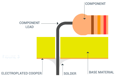
When it comes to assembling PCBs, Through-hole technology (THT) or through-hole assembly is a common mounting scheme utilized for electronic components. This technique involves inserting the leads of components into holes drilled into the PCB, and soldering them to pads on the opposite side. THT has largely replaced previous assembly methods, such as point-to-point construction. From the 1950s, with the emergence of second-generation computers, to the late 1980s, when surface-mount technology (SMT) became popular, nearly all components on a typical PCB were through-hole components.
Initially, PCBs only had printed tracks on one side, then later, both sides. Multilayer boards were also eventually introduced. In order to make contact with required conductive layers, through-holes were plated, creating Plated Through Holes PTH. While plated-through holes are no longer necessary for making component connections with SMT boards, they are still utilized for interconnections between layers, commonly referred to as “vias”.
Although SMT has overtaken THT as the leading technology for PCB assembly manufacturing, THT is still in use today, particularly for boards requiring through-hole components, like antennas, DC jacks, and wires.
What are some strategies for reducing the cost of PCB with through holes?
To minimize your PCB cost, it is important to consider the design of the holes, annular rings, and hole density. One option is to use larger holes and annular rings, as small holes require high precision machines that can incur additional charges. It is also important to keep in mind the minimum annular ring requirement for through hole pads and vias to avoid increased PCB costs.
Using larger annular rings has the additional benefit of increasing PCB quality by reducing drilling tolerance or shaving rings. Additionally, reducing hole density per square meter can help to decrease drilling time and associated costs.
To determine the added cost of smaller hole sizes and minimum annular ring requirements, it is best to contact the PCB fabricator directly for information on their policies regarding additional charges for standard printed circuit boards. By considering these factors in your PCB design, you can potentially reduce your overall PCB cost.
Design Guidelines for Through Hole
Through hole components can be used alongside SMT components on a printed circuit board. It is important to take note of some design guidelines to ensure successful assembly of through hole components. Below are some of the guidelines to consider:
Soldering:
Through-hole components are often attached to a printed circuit board using a wave soldering system. This process involves passing the circuit board over a molten solder, which is forced into the through-hole to form a strong solder joint. It is important to ensure that SMT components are not placed on the back of the PCB during this process, as the assembler will need to block off the area around SMT components to prevent them from being exposed to the molten solder. Alternatively, through-hole parts can be manually soldered.Footprints:
It is important to use the correct footprint dimensions recommended by the part manufacturer. This helps to ensure that the circuit board is easily assembled. While some components, such as through-hole resistors, can make use of differently spaced holes, it is important to note that most components cannot.Spacing:
Proper spacing is crucial when soldering through-hole parts. When components are spaced correctly, it enhances automated soldering systems. It is also important to note that larger through-hole parts can overshadow SMT parts and prevent them from being soldered properly. Therefore, allowing enough space between parts is important for manual rework.Hole size:
It is necessary to use the hole size recommended for the part’s lead diameter. Very large through holes will not accommodate the molten solder, which can lead to poor solder joint. On the other hand, too small holes will not allow you to insert the lead of the part. Therefore, it is important to use the recommended hole size to ensure successful assembly of through hole components.
In conclusion, through hole components will still be in use for a while, therefore, it is important to take note of the above design guidelines for successful assembly of through hole components. Additionally, it is crucial to ask the manufacturer about part placement to prevent any assembly issues.
Notes for Through-hole Components Design
Through-hole components still have their uses in printed circuit board design despite the popularity of surface mount parts. When designing with through-hole components, there are several considerations to keep in mind.
Firstly, for power components, through-hole connections can provide thermal and mechanical stability, which is beneficial and sometimes necessary. The soldering process for larger SMT parts can be complex due to the amount of metal needed to go through heat.
Secondly, through-hole pins can offer greater strength and are beneficial for interfacing with parts such as switches and connectors. On the other hand, SMT connectors can be more prone to being ripped from their pads if their mating connector is unplugged with force.
Lastly, for high-temperature parts, plated through holes are generally better conductors and can offer better thermal management than surface mount parts. These parts are often bolted onto the PCB for added stability and heat dissipation. It’s important to use the correct hole size and spacing recommended by the component manufacturer and provide enough space for manual repairs during assembly. Using too small or too large holes can lead to poor soldering quality and possible damage to the component.
FAQs
Why is plated through hole important?
PTHs are important in PCBs because they enable the electrical connectivity between the different layers of the board. Without PTHs, it would be very difficult to interconnect the layers of a PCB. PTHs allow for efficient transfer of signals across different layers, which is necessary for many electronic devices that require multiple circuits to work together. PTHs also add structural support to the board and can help manage heat dissipation, which is essential for devices that generate a lot of heat.
How to distinguish PTH from NPTH?
PTH, or Plated-Through Hole, is a type of hole in a PCB substrate that has been drilled and plated with a conductive material to provide electrical connectivity between different layers of the board. NPTH, or Non-Plated Through Hole, is a hole in the PCB substrate that has not been plated, and therefore does not provide electrical connectivity between different layers.
One way to distinguish PTH from NPTH is to inspect the holes closely. PTHs will have a metallic coating that extends down into the hole, whereas NPTHs will have an exposed substrate. Another way to distinguish between PTHs and NPTHs is to look at the design files for the PCB. PTHs will be denoted as plated holes in the design files, while NPTHs will be denoted as non-plated holes. Finally, a continuity test with a multimeter will indicate conductivity in PTHs, while NPTHs will show an open connection.
What is NPTH (Non-Plated Through Hole) used for?
NPTH stands for Non-Plated Through Hole. As the name suggests, NPTH is a type of hole on a printed circuit board that is not plated with metal.
NPTH holes are typically used for mechanical purposes such as mounting components or providing access to a specific part of the board. They're also sometimes used to reduce the number of required plated through holes that can increase the cost of manufacturing.
Unlike plated through holes (PTHs), which are designed to facilitate the flow of electric current between layers of a PCB, NPTHs are not designed to carry electrical signals. Plated through holes are lined with a conductive layer that connects the top and bottom layers of a PCB, allowing current to pass through.
What is Via in PCB?
A via in a PCB is a hole that is plated with metal, which connects the conductive layers of a PCB. Vias enable a signal or power to be routed from one layer of a PCB to another.
Vias are used to connect the different layers of a PCB, which is important because modern PCB designs can have many layers. For example, a four-layer PCB might have two internal layers that provide a ground and power plane, respectively, with traces running on the outer layers. Without vias, it would be difficult to connect these internal layers to the outer layers, making it more challenging to route the necessary signals and power lines.
Vias come in different sizes and shapes, depending on the design of the PCB, and are fabricated using specialized equipment. When a via is created, a hole is drilled through the PCB and then coated with a conductive layer (usually copper). Vias can be used for both through-hole and surface mount components, and are an essential part of modern PCB design.
What is blind via hole in PCB?
A blind via hole in PCB is a via hole that extends from the surface of one layer of the board to an internal layer, but does not go all the way through to the opposite surface of the board. Blind vias are used to connect a component or trace on an outer layer of the board to an inner layer, while minimizing the size and number of vias on the outer layer, which can help reduce the overall size and weight of the board. They are very useful in high-density PCB designs where space is at a premium.
What is Buried Via Hole in PCB?
A buried via hole in PCB is a via hole that connects two or more inner layers of the board without coming out at any of the board surfaces. Buried vias are used to make connections within the board while avoiding any interference with the outer layers and can also help reduce the number of vias needed on the outer layers, which can help improve the overall reliability and performance of the board. They are commonly used in high-density multi-layer PCB designs where space is limited and signal integrity is critical.
What types of vias in PCB?
There are several different types of vias used in PCBs, including:
Through-hole via (TH): A via that starts from the top layer of the PCB and goes all the way through to the bottom layer.
Blind via: A via that starts on the surface of the PCB and only goes to an internal layer of the board, but does not go through to the other side of the board.
Buried via: A via that starts and ends within the internal layers of the board, and does not connect to any outer layer.
Micro via: A very small via, typically with a diameter of less than 0.15mm.
Via-in-pad: A type of via that is located directly in the pad of a surface mount component. This allows for a more compact design and is useful for high density PCBs.
Each type of via has its own advantages and disadvantages, and it's important to choose the right type for your specific application.
Why Do Plated Through Holes Fail?
The failure of PTHs is often caused by cracks in the copper plating within the hole, which is commonly known as barrel fatigue. This is due to the difference in CTE values between the copper plating (17 ppm) and the PCB board (70 ppm). To ensure a reliable PTH, it is essential to consider factors such as proper architecture (including height and diameter), material CTE, and plating thickness and material. Insufficient plating thickness can result from inadequate current or time in the copper plating bath. IPC provides guidelines for the Round Robin Reliability Evaluation of Small Diameter PTHs (less than 20 mil) in its IPC TR-579 document.
What are the test methods to verify the reliability of PTH?
- Modeling and simulation
- Cross-sectioning + solder float/shock
- Thermal shock testing (also thermal cycling)
- Interconnect stress testing (IST)
- Printed Board Process Capability, Quality, and Relative Reliability (PCQR2)
- Highly Accelerated Thermal Shock (HATS)
What is the minimum diameter of the through hole?
The minimum diameter of a through-hole via in a PCB depends on several factors, including the capabilities of the PCB fabrication and assembly process and the electrical requirements of the board.
In general, the minimum diameter of a through-hole via is often around 0.25mm (10 mils) for standard PCBs. However, smaller diameter vias can be achieved using more advanced techniques and equipment. For example, laser drilling can produce vias with a smaller diameter of around 0.1mm (4 mils) or less.
It is important to note that smaller vias typically require more advanced manufacturing techniques and come at a higher cost. So the selection of the minimum via diameter should balance the cost and functionality requirements of the PCB.
What is PCB Countersink Holes ?
PCB countersink holes are holes on a printed circuit board that are widened at the top to accommodate the head of a screw or bolt. These holes are often used to mount the PCB to another surface, as the screws recess into the PCB, allowing for a flush fit. Countersink holes are especially useful when you want to avoid having protruding screw heads, which could interfere with other components or structures.
What is Castellated Mounting Holes in PCB?
Castellated mounting holes are a type of PCB through-hole technology. They are essentially half holes along the edge of a PCB. These half holes are cut in a particular pattern with alternating fingers and notches, resembling the battlements on a castle wall hence the name "castellated". They are used to create a connection between the PCB and another device or circuit board through the tab of the exposed, non-plated pad
Castellated holes are often used for surface-mount applications, where they allow components to be connected to both sides of the PCB. Additionally, they provide a stable mechanical connection to a mating socket or board, allowing for easy replacement or repairs if necessary. Castellated holes are sometimes referred to as castellations or half holes.
What is Half Hole PCB?
Half hole PCB, also known as castellated PCB, is a variation of PCB manufacturing that involves creating holes on the edges of a PCB. These holes are drilled partially through the board, leaving a small amount of copper on both sides, which resembles a castle turret, hence the name "castellated". Half holes can be used to create a smaller footprint for surface mount components, allowing them to be mounted on the edge of a PCB. Half holes can also be used to create a stronger mechanical connection between two PCBs or to create a breakout board for easy testing of soldered devices.


