


Your Trusted Prototype PCB Manufacturing And Assembly Partner.
When you partner with us, we do everything to ensure your PCB manufacturing and assembly are completed on time to your specifications with the highest quality.
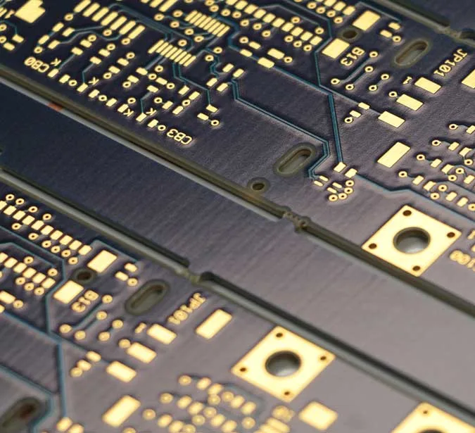
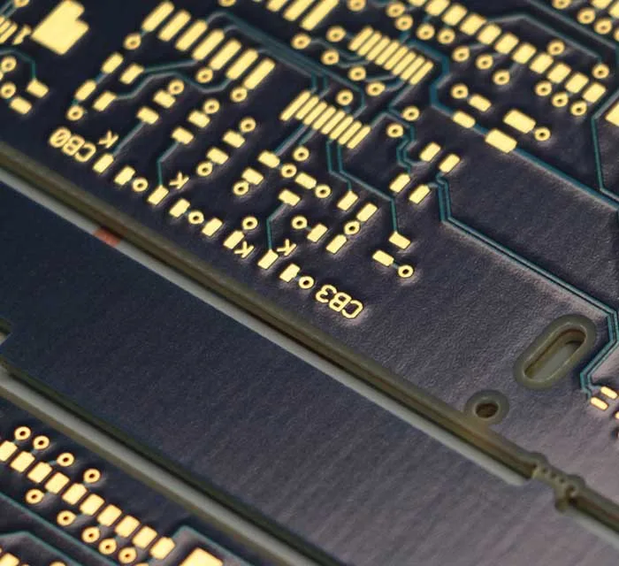
Leading manufacturer of PCB Fabrication and Assembly in China.
Multilayer PCBs, also known as multi-layered printed circuit boards, are PCBs that have multiple layers of conductive traces and insulating material. The layers are laminated together to form a single board, which can be used for various applications. One of the most popular types of multilayer PCBs is the 4-layer PCB, 6-layer PCB, and 8-layer PCB.
A 6-layer PCB has six layers of conductive and insulating material, making it an ideal choice for complex circuit designs requiring high-density interconnects. The additional layers provide increased routing flexibility and reduce the need for extensive use of vias. Additionally, 6-layer PCBs have a smaller footprint than other types of PCBs, making them a preferred choice for products that require a compact design.
A 6 layer PCB, also known as a six-layer printed circuit board, is a type of multilayer PCB that consists of six layers of conductive material separated by insulating material. The layers are bonded together with heat and pressure to form a single circuit board. Each layer can contain traces, vias, and components, which are interconnected to form a complete circuit.
6 layer PCBs are commonly used in complex circuits that require high-density interconnects, such as telecommunications equipment, computers, and consumer electronics. They offer several advantages over other types of PCBs, such as increased routing flexibility, reduced need for vias, and a smaller footprint. They also allow for a higher number of components to be included in the circuit design, which makes them a preferred choice for high-speed signal transmission applications.
A 6 layer PCB is used in a wide range of electronic applications. 6 layer PCBs offer several advantages over other types, such as increased routing flexibility, reduced need for vias, and a smaller footprint. These advantages make 6 layer PCBs a preferred choice for high-speed applications, such as telecommunications equipment, computers, and consumer electronics.
Advantages of 6 Layer PCB:
The design process for a 6-layer PCB involves stacking and layer arrangement, layout and routing design, component placement and pad design, and impedance control and signal integrity design. By following these steps, the PCB design can meet the necessary requirements and meet the demands of high-speed applications.
PCB Stacking and Layer Arrangement: The first step in designing a 6-layer PCB is to determine the stacking and layer arrangement of the PCB. Different stacking configurations can be selected depending on the design requirements and the number of required signals. For example, it is common to place the ground and power layers internally and signal layers on the top and bottom layers.
PCB Layout and Routing Design: During the PCB layout and routing design phase, considerations must be given to component dimensions, placement, and signal transmission paths. PCB design software can be used to create the layout and routing, and it is important to follow PCB design specifications and standards.
PCB Component Placement and Pad Design: In the PCB component placement and pad design phase, components are placed on the PCB and their distance and position are determined. Additionally, component pads must be designed to secure the components onto the PCB.
PCB Impedance Control and Signal Integrity Design: During the PCB impedance control and signal integrity design phase, it is crucial to ensure that the PCB design meets signal integrity requirements and control impedance. This typically involves using impedance control tools such as differential pairs, matched trace lengths, and impedance matchers.
Tips for 6 Layer PCB Design Process
PCB Board Thickness and Material Selection: The choice of PCB board thickness and material selection is important for a 6-layer PCB design. The board thickness will depend on the size and complexity of the design, as well as the mechanical and electrical requirements of the application. Common materials for a 6-layer PCB include FR-4, high-frequency, and specialty materials.
PCB Board Edge Treatment and Protection Design: The PCB board edge treatment and protection design are important considerations in the design process. The edges of the PCB should be smooth and free from any burrs or sharp edges that could cause injury or damage to the board during handling. Additionally, protection design can include the use of conformal coatings or edge plating to protect the board from environmental factors such as moisture or dust.
PCB Special Process Design, such as Blind Via and Impedance Control: A 6-layer PCB design may require special processes such as blind vias and impedance control. Blind vias are used to connect inner layers to the surface layers of the PCB without passing through all layers. Impedance control involves designing the trace widths, spacing, and thickness to ensure a consistent impedance throughout the board, which is important for high-speed applications.
There are several types of 6-layer PCB stack ups available, and the choice of the best one depends on the specific requirements of the design. Each stack up has its advantages and disadvantages and is suitable for different applications. Here are some common types of 6-layer PCB stack ups:
Standard Stackup: This is the most basic 6-layer PCB stack up, consisting of two outer signal layers, two inner signal layers, and two power or ground planes in the center. This stack up is suitable for simple designs with low-speed signals.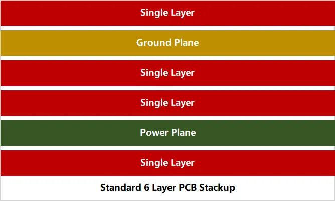
Signal-Plane-Plane-Signal (SPPS) Stackup: This stack up is useful for high-speed designs where signal integrity is critical. It consists of two outer signal layers, two internal ground planes, and two power planes adjacent to the ground planes. The internal power planes provide power distribution, and the ground planes provide shielding and reduce electromagnetic interference (EMI) noise. This stack up provides good signal quality by having a ground plane adjacent to each signal layer.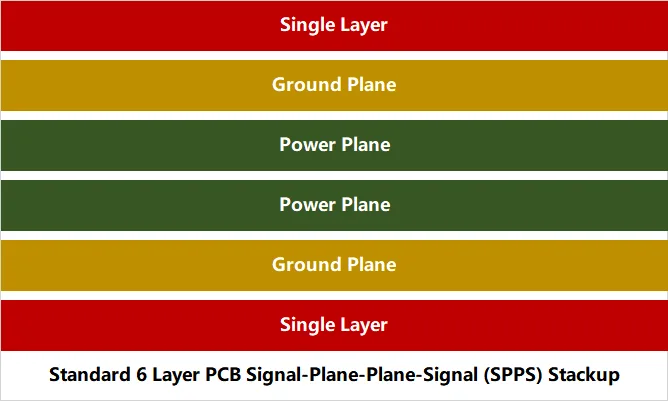
Power-Plane-Signal-Plane-Power (PPSP) Stackup: This stack up is used in designs where power integrity is critical. It consists of two outer signal layers, a power plane, a signal layer, another ground plane, and another power plane. The power planes provide power distribution, and the ground planes provide shielding and reduce EMI noise. This stack up provides good power distribution by having two power planes on either side of a signal layer.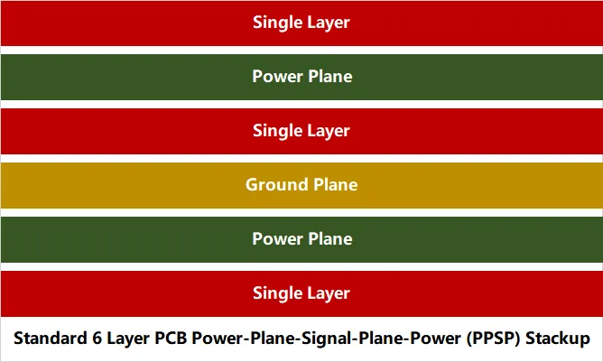
Mixed Signal-Plane-Plane-Mixed Signal (MSPPMS) Stackup: This stack up is used in designs where both high-speed and low-speed signals are present. It consists of two outer mixed signal layers, two internal ground planes, and two power planes adjacent to the ground planes. The internal power planes provide power distribution, and the ground planes provide shielding and reduce EMI noise. This stack up provides good signal quality by having a ground plane adjacent to each signal layer.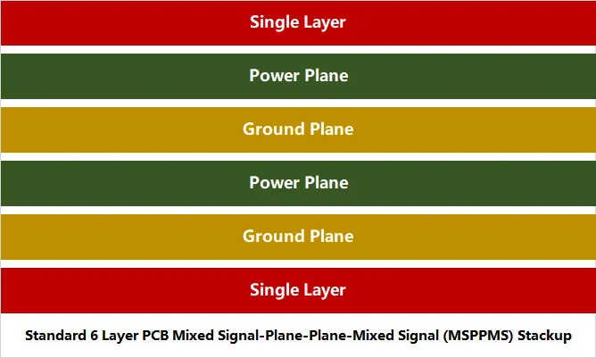
Which one is the best 6 Layer PCB Stackup?
The best 6-layer PCB stack up depends on the specific design requirements. For example, a SPPS stack up may be best for a design with high-speed signals, while a PPSP stack up may be best for a design with high power requirements. Mixed signal designs may benefit from a MSPPMS stack up. The selection of the best stack up should be based on a thorough analysis of the design requirements, including signal frequency, signal quality, power distribution, and EMI noise reduction.
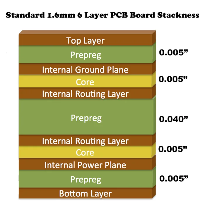
The thickness of a 6-layer PCB stackup can vary depending on the design requirements and materials used. However, a typical 6-layer PCB stackup might have the following thicknesses:
This results in a total thickness of approximately 1.05 mm (41 mil). However, the actual thickness can vary based on the specific materials used and the manufacturing process. It’s important to work with your PCB manufacturer to determine the appropriate stackup thickness for your design requirements.
Fabrication of 6 layers of PCB might sound easy but it’s a complex process.
Here is a step-by-step process of the manufacturing process of a six-layer PCB:
Material Selection: The next step is to select the appropriate materials for the PCB, including copper foil, core materials, and prepreg.
Inner Layer Core Preparation: The core material is laminated with copper foil on both sides. This is done by using a lamination press at high temperatures and pressure.
Image Transfer: The inner layer of the PCB is then coated with photoresist, exposed to ultraviolet light, and developed. This process transfers the PCB design onto the copper layer.
Etching: The unwanted copper is then etched away using a chemical solution, leaving only the desired circuitry.
Drilling: Holes are then drilled into the PCB for components and interconnections. The holes are plated with copper to make them conductive.
Plating: The entire board is plated with a thin layer of copper, including the walls of the drilled holes. This is done to provide a conductive path between the layers.
Outer Layer Imaging: The outer layer of the PCB is coated with photoresist and the desired circuitry is transferred onto the copper layer using ultraviolet light and development.
Etching and Stripping: The unwanted copper is etched away using a chemical solution, leaving only the desired circuitry. The photoresist is then stripped away.
Solder mask Application: A layer of solder mask is applied to protect the copper traces and prevent solder bridges during assembly.
Silkscreen Printing: Component outlines, labels and other markings are printed onto the PCB surface.
Surface Finish: The PCB surface is coated with a surface finish such as HASL (Hot Air Solder Leveling) or ENIG (Electroless Nickel Immersion Gold) to protect the copper and facilitate soldering.
Electrical Testing: Finally, the finished PCB is electrically tested to ensure that all connections are working correctly.
JHYPCB is a PCB manufacturer in China that offers low-cost PCB manufacturing services, including 6-layer PCB prototype service. This service allows you to obtain a 6-layer PCB prototype at a relatively low cost, enabling you to test and evaluate your design to ensure that it meets your requirements. At JHYPCB, you can easily obtain an instant quote for 6-layer PCB prototype manufacturing using their online quoting tool by entering your PCB design specifications such as size, layer count, and quantity. Prices may vary due to various factors but are typically under $1000. Additionally, JHYPCB offers fast delivery services, allowing you to receive your 6-layer PCB prototype in a week or less, enabling you to test and validate your product faster and get it to market sooner. Overall, JHYPCB’s 6-layer PCB prototype service is a cost-effective, efficient, and convenient option.
As a reliable PCB manufacturer, we offer multi-layer PCB fabrication services, including 6-layer PCB fabrication service. Our 6-layer PCB fabrication service utilizes the latest technology and equipment to ensure high-quality, high-precision PCB fabrication. We have an experienced team and excellent manufacturing processes that can provide perfect 6-layer PCB fabrication services for customers. We offer various options to meet different needs, such as controlling the board thickness, PCB material, trace width, and other parameters to meet different circuit requirements. Additionally, we offer customized 6-layer PCB fabrication services to tailor PCB designs to the unique needs of our customers. We understand that time is crucial for our customers, so we have made significant efforts to ensure fast delivery to ensure customers receive the required 6-layer PCBs on time. If you are looking for high-quality and reliable 6-layer PCB fabrication services, we are your best choice.
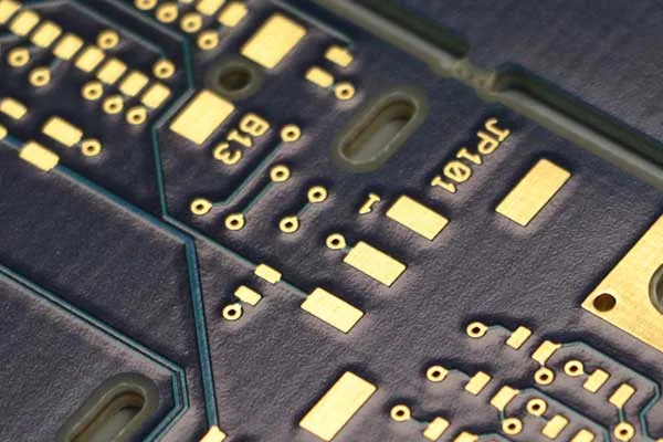
We provide high-quality 6-layer PCB fabrication services, including a 1.6mm 6 layer PCB fabrication. We are the ideal choice for all your 6-layer PCB fabrication needs.
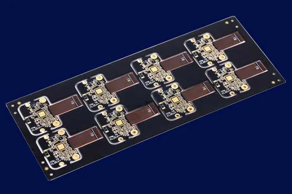
We offer 6-layer rigid flex PCB fabrication service. Our PCB manufacturing experience allows us to provide you with high-quality 6-layer rigid flex PCB fabrication services.
We offer a 6-layer PCB motherboard manufacturing service aimed at providing customers with high-quality and reliable PCB solutions.
We offer a 6-layer High Density Interconnect (HDI) PCB manufacturing service aimed at providing customers with high-quality and reliable HDI PCB solutions.
A 6 layer PCB is a printed circuit board with 6 layers of conductive material separated by layers of insulating material. It is used in a wide range of electronic applications to provide increased functionality and better signal integrity.
A 6 layer PCB provides several advantages, including increased circuit density, better signal integrity, and reduced electromagnetic interference. It also allows for more complex circuits and provides better thermal management.
The materials used to make 6 layer PCBs include copper, fiberglass or other composite materials for the insulating layers, and soldermask and silkscreen for the top and bottom layers.
Design considerations for 6 layer PCBs include layer stackup, trace width and spacing, via placement, and component placement. It is important to ensure that the design meets the required specifications and that it is manufacturable.
6 layer PCBs are used in a wide range of electronic applications, including telecommunications, computing, automotive, and medical devices.
Yes, 6 layer PCBs can be customized to meet specific design requirements and specifications. Customization may include layer stackup, material selection, and component placement.
The turnaround time for manufacturing 6 layer PCBs varies depending on the complexity of the design and the manufacturer's production capacity. It typically ranges from a few days to a few weeks.
The cost of a 6 layer PCB is determined by several factors, including the size and complexity of the design, the number of layers, the materials used, and the manufacturer's pricing structure.
The minimum trace width and spacing for 6 layer PCBs depends on the manufacturer's capabilities and the design requirements. It is typically in the range of 4 to 6 mils.
The minimum drill size for 6 layer PCBs depends on the manufacturer's capabilities and the design requirements. It is typically in the range of 6 to 8 mils.
When you partner with us, we do everything to ensure your PCB manufacturing and assembly are completed on time to your specifications with the highest quality.
Fill out the form below, and we will get back to you within the next 24
hours to complete the order, and then you’re all set to get started!