Double sided PCBs: The Introduction
Double-layer printed circuit boards are one of the most common types of PCBs used today. As their name suggests, these boards have conductors on two layers with an insulating dielectric material in between. This basic two-layer construction makes double-layer PCBs an affordable option suitable for a wide range of applications.
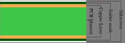
Double-layer PCBs are composed of a non-conductive substrate material, typically FR-4 fiberglass, with a layer of copper laminated to each side. The two thin sheets of copper act as the conductive layers for tracing circuits and mounting components. The simple sandwich structure strikes a balance between complexity and functionality for many electronics projects.
Compared to boards with additional layers, double-layer PCBs provide enough flexibility for routing different signals while maintaining a straightforward layout. They can accommodate everything from simple hobby electronics to commercial products like consumer appliances, IoT devices, instruments, and other equipment with low-complexity circuits. For applications that don’t require advanced multifunctionality, double-layer boards offer an optimal blend of capabilities and cost-effectiveness.
The modest design needs of double-layer PCBs make them easier to learn for beginners compared to multilayer boards. They also simplify the modification process for iterative prototyping or when adjustments are needed down the road. At the same time, the two-layer structure retains sufficient options for trace routing schemes to avoid interference and crosstalk issues.

How we connect our double layer PCBs
As a leading manufacturer of the best double-layer PCB boards in the market, our products feature innovative board connection technologies. The components on the two board sides are connected by using the through-hole or surface-mount technology. The connection method depends on the needs of the product being manufactured. This is why we have a wide range of board connection technologies. Double-layer PCB boards feature all the original layers that come with the single-sided PCBS such as the solder mask, the silkscreen, the copper layer, and the substrate. Except that these layers are featured on both sides of our double-layer PCB boards.
Double sided PCBs: Applications
Double-sided board applications can be limitless. It is important to note that our Multilayer PCB boards help create both existing and new electronic products. Multilayer circuit boards feature a perfect finish that is characterized by fine line mounts, solder coated, a good quantity of copper build, and a super rich finish. Our double-sided PCB boards can be used for a wide range of applications such as:
- Vending machines
- Traffic systems
- Amplifiers
- Test equipment
- Line reactors
- Automotive dashboards
- Power monitoring systems
- Phone systems
- Printers
- Hard drives
- LED lighting
- HVAC equipment
- Power conversion components
- UPS systems
- Regulators
- Instrumentation
- Control relays
- Converters
- Power supplies
- Industrial controls, and many more.
Benefits and Advantages of double layer PCBs
Double-layer PCBs offer several advantages that explain their widespread use in electronics design and manufacturing. Here are some of the top benefits of selecting double-layer PCBs:
- Cost-Effective Solution
With only two copper layers, double-layer boards require fewer manufacturing steps compared to multilayer boards. This makes them significantly more affordable to produce while still providing enough functionality for many applications. For budget-conscious projects, double-layer PCBs deliver value. - Simplified Layout and Routing
The two-layer structure of double-layer boards simplifies the layout and trace routing process. With fewer layers, designers have less complexity to manage. This makes the design stage more accessible for new engineers and faster for experienced designers. - Ideal for Basic Circuits
For simple, low-component count circuits without advanced functionality needs, double-layer PCBs are usually the ideal fit. The two layers provide enough flexibility to route different signals effectively on a budget. Multilayer boards would be overkill. - Easier Repairs and Modifications
Compared to dense multilayer boards, double-layer PCBs are easier to modify or repair post-production. Their simplicity leaves more opportunities to make adjustments by cutting traces or soldering new jumper wires. - Flexibility in Trace Routing
While not as flexible as 4+ layer boards, prudent trace routing on double-layer PCBs can reduce interference. Strategies like running matching impedance traces on opposite sides or crossing perpendicular help.
On the whole, the balanced capabilities of double-layer PCBs make them a versatile and affordable choice suitable for a wide range of non-complex circuit needs. Their advantages explain why double-layer boards remain a mainstay of electronics design.
Layout and design basics for double layer PCBs
When laying out circuitry and routing traces for a double layer printed circuit board, designers should follow a few key principles and strategies. Here is an overview of double layer PCB layout fundamentals:
- Typical Construction
The core of a double layer board consists of a non-conductive substrate like FR-4 fiberglass with a thin copper layer bonded to each side. The two copper layers act as conductive surfaces. - Connecting Components
Components and integrated circuits get electrically connected via copper traces etched into the conductive layers. Traces transmit signals between mounts. - Minimizing Noise
With only two layers, paying attention to trace routing helps minimize noise. Techniques like running matching signals on opposite sides or crossing traces perpendicularly reduces interference. - Via Usage
For traces that need to switch layers, vias or through-holes filled with conductive material can make the connection through the substrate. Minimizing vias helps. - Component Placement
Strategic component placement based on connection needs optimizes routing by reducing trace lengths and complexity. Group related circuit sections. - Balancing Trace Lengths
When routing signals for components like capacitors or resistors, balancing trace lengths helps maintain signal integrity. Consider impacts of etch and tolerances.
By following layout guidelines and best practices, double layer PCBs can accommodate well-designed circuits. The key is using the two conductive layers strategically.
Manufacturing process for double layer PCBs
The fabrication of double layer printed circuit boards involves a number of key steps to produce the layered structure with circuit traces. Here is an overview of the double layer PCB manufacturing process:
- Bonding Base Layers
The process starts with the raw PCB substrate, typically FR-4 fiberglass. Copper foil gets laminated to both sides to form the conductive layers. - Applying Photoresist
A photosensitive coating called photoresist gets applied to the copper surfaces on both sides. This will be used to transfer the trace pattern. - Exposing Circuitry Pattern
Next, the board gets exposed to UV light through a mask with the desired circuit trace layout. Exposed photoresist hardens. - Etching Copper
The PCB then goes through an etching bath to remove excess copper not hardened by UV exposure. This leaves just the traced circuitry. - Removing Photoresist
Once etching is complete, the remaining photoresist gets stripped away, leaving the finished conductive pattern on both layers. - Testing and Finishing
The fabricated board now undergoes testing before final finishing steps like legend printing, solder mask application, and protective coatings.
With quality standards checks throughout, this multilayer process efficiently produces completed double layer PCBs ready for component assembly.

What to look for when choosing a double layer PCB manufacturer
Since double layer boards are a fundamental PCB type, selecting a reliable board manufacturer is key. Here are important factors to consider when choosing a partner for double layer PCB fabrication:
- Proven Capabilities
Look for demonstrated experience with high-volume double layer PCB production using latest equipment and processes. This ensures they can deliver quality. - Rigorous Testing
The manufacturer should have rigorous quality control testing throughout fabrication. This includes verifying trace widths, alignment, laminate integrity, etc. - Design File Checking
A thorough design rule check on the Gerber files is needed to catch any errors before production begins. This prevents faulty boards. - Lead Time Management
On-time delivery is crucial, so evaluate their supply chain practices, inventory and production bandwidth to meet lead time commitments. - Responsive Communication
A responsive, communicative partner will collaborate with you through every production stage and address any issues promptly. - Cost Transparency
Beware of hidden fees – a good manufacturer will provide clear, detailed pricing with no surprise charges for rework, testing or other standard procedures.
By thoroughly vetting manufacturers against benchmarks like these, you can select a double layer PCB partner you can trust for producing quality boards delivered on time.
Conclusion
In summary, double layer printed circuit boards offer an optimal balance of affordability, ease of design, and functionality for a wide range of electronics applications. Their two-conductor-layer construction provides enough flexibility for routing low-complexity circuits without the complexity and costs of multilayer boards.
For hobbyists, startups, and budget-minded projects, double layer PCBs are often the right choice to deliver capable performance without breaking the bank. Their simplicity also makes them ideal for teaching new electrical engineers PCB layout and routing basics. Even with the growing capabilities of multilayer boards, double layers remain popular for many consumer, commercial, and industrial uses.
When designed thoughtfully, double layer boards can accommodate most non-complex circuit needs. As PCB fabrication technology continues advancing, capabilities of two-layer boards will also improve further. The future looks bright for this tried and true PCB variety that strikes the right tradeoffs.
With the right manufacturer partner providing quality production and testing, electronics designers can rely on double layer PCBs as a versatile and enduring solution for a wide array of applications. Their advantages will ensure these specially fabricated boards remain core to electronics projects and products for years to come.
Contact us for more benefits of our innovative double sided PCBs
If you need to know various other features and benefits of our double sided boards, you can contact us. We will give you a lot of information about how our PCBs can be suited to your manufacturing projects and advanced electronic products. Our products come with increased circuit density, advanced complex designs, and reduced costs. Our double sided boards offer manufacturers and customers the perfect base material to create that next ground-breaking electronic product. Contact our team of experienced experts to talk more about your needs.
Get a quote for our double sided boards
You can also contact us to get quotations for the double sided boards. To get an accurate quote for your project, you can use the Multilayer PCB assembly/fabrication quote request form. This way, you can easily submit the right information about your project needs. If you need both Multilayer PCB assembly and Multilayer PCB fabrication, then you can submit the request for a quote as separate forms. You can also choose to send us your BOM and Gerber files via email at sales@pcbjhy.com. You can also call us at +86 13825274100 if you need further information concerning our Multilayer PCB products and services.
Why choose us?
Customers all over the world choose us for various reasons. We an industry-leading PCB manufacturing brand that has been in the business for many years. Through decades of dedicated service to quality PCB manufacturing, we have been able to build a reputation as the best trustworthy and most reliable PCB manufacturer.
Whether you need double sided PCB design or a board prototype, we are your most reliable option. We combine a large and sophisticated manufacturing plant with advanced PCB expertise to cater to all the needs of our PCB customers. You get our promise that the PCBs will be produced and delivered on time at all times. When it comes to PCB manufacture and prototyping, you can expect to get the best turnaround times from us. Without compromising service and quality, you can expect to get the best solutions from us when it comes to double sided boards.
Related Reading: