


Your Trusted Prototype PCB Manufacturing And Assembly Partner.
When you partner with us, we do everything to ensure your PCB manufacturing and assembly are completed on time to your specifications with the highest quality.
Leading manufacturer of PCB Fabrication and Assembly in China.
An 8 layer PCB is a type of multilayer printed circuit board that consists of eight layers of conductive material separated by insulating layers. These layers are used to connect different components of an electronic circuit, and they offer greater flexibility and efficiency than single or double-sided PCBs.
There are other types of multilayer PCBs such as 4 layer, 6 layer, and even up to 100 layers. The number of layers in a PCB depends on the complexity of the circuit design and the performance requirements of the electronic device it will be used in.

JHYPCB is a leading manufacturer of high-quality multilayer PCBs, including 4 layer, 6 layer, 8 layer, and even up to 64 layer PCBs. We provide comprehensive PCB manufacturing services from design and prototyping to full-scale production, testing, and assembly.
Our experienced team of engineers and technicians use the latest PCB manufacturing equipment and techniques to ensure that all of our multilayer PCBs meet the highest standards of quality, reliability, and performance. We offer a wide range of materials and technologies to suit different applications and specifications, and we work closely with our customers to customize their designs and optimize their PCBs for cost and performance.
Whether you need a small batch of prototypes or a large volume of production PCBs, JHYPCB can provide the right solution for your needs. Our multilayer PCB manufacturing services are backed by our commitment to quality, on-time delivery, and customer satisfaction. Contact us today to learn more about how we can help you with your multilayer PCB needs.
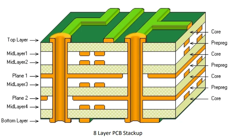
An 8 layer PCB stack up refers to the arrangement of the eight layers that make up a multilayer printed circuit board. The layers are stacked together in a specific order, with each layer serving a specific purpose in the circuit design.
Typically, an 8 layer PCB stack up consists of four signal layers, two power planes, and two ground planes. The signal layers are used to route signals between components, while the power and ground planes provide a stable voltage and current distribution throughout the board.
The stack up order can vary depending on the specific requirements of the PCB design, but a common order for an 8 layer PCB stack up is:
The ground and power planes are typically placed adjacent to signal layers to provide better signal integrity and reduce noise. The use of multiple power and ground planes also helps to reduce electromagnetic interference (EMI) and improve the overall performance of the circuit.


The specific details of an 8 layer PCB stack up can be customized based on the specific requirements of the PCB design, such as signal speed, impedance, and power requirements.
Design and engineering: The first step is to create a detailed design for the PCB using computer-aided design (CAD) software. The design must consider factors such as the number of layers, the dimensions of the board, the placement of components, and the routing of signals.
Preparing materials: Once the design is finalized, the manufacturing process begins by preparing the materials. This includes cutting and cleaning the copper-clad laminate sheets to the required size and thickness.
Inner layer imaging: In the next step, a photoresist layer is applied to the copper-clad laminate sheets. This layer is then exposed to ultraviolet light through a photomask, which transfers the pattern of the PCB design onto the photoresist.
Etching: After imaging, the copper is chemically etched away from the exposed areas, leaving behind the circuit pattern. This process is repeated for each inner layer of the PCB.
Lamination: Once all the inner layers have been imaged and etched, they are laminated together using a heat and pressure process. This creates a solid, layered board with alternating layers of copper and insulating material.
Drilling: Next, small holes are drilled into the board at specific locations to create vias, which are used to connect the different layers of the board.
Plating: The vias are then plated with a conductive material, typically copper, to create a continuous electrical connection between the layers.
Outer layer imaging: The top and bottom layers of the PCB are then imaged and etched, following the same process as the inner layers.
Solder mask and silkscreen: Once the circuit pattern is complete, a solder mask layer is applied to protect the copper traces from oxidation and contamination. A silkscreen layer is also applied to print component designations and other markings on the board.
Finishing: Finally, the board is finished with a protective coating, such as gold plating or immersion tin, to protect the copper traces and vias from corrosion and ensure long-term reliability.
After the manufacturing process is complete, the PCB is inspected and tested for quality assurance before it is shipped to the customer.
The materials and techniques used to manufacture 8-layer PCBs are similar to those used for other multilayer PCBs, but higher quality materials and more advanced techniques are required due to the higher requirements and complexity of 8-layer PCBs.
Here are common materials and techniques used to manufacture 8-layer PCBs and their impacts on PCB performance:
Raw materials: High-quality raw materials such as high-TG glass fiber reinforced materials and high-frequency low dielectric constant materials are required to manufacture 8-layer PCBs. These materials have higher temperature resistance, flame resistance, and durability to ensure the long-term stability and reliability of the circuit board.
Surface finishes: Surface finishes protect the copper layer of the circuit board from oxidation and corrosion. Metal chemical deposition (MPC) is a popular surface finish technique that provides excellent impedance control and signal integrity.
Lamination techniques: Lamination techniques are critical for manufacturing 8-layer PCBs. This technique uses heat and pressure to laminate different layers together to form a continuous circuit board. Different lamination techniques can affect the accuracy and stability of the circuit board.
Through-hole technology: Through-hole technology is used to establish electrical connections between different layers. Using high-quality through-hole technology can reduce signal distortion and crosstalk.
Encapsulation materials: Encapsulation materials can affect the physical and chemical properties of the circuit board, such as elastic modulus, thermal expansion coefficient, and bonding strength. Choosing high-quality encapsulation materials can ensure the long-term stability and reliability of the circuit board.
In summary, the selection of materials and techniques for 8-layer PCBs is crucial to PCB performance. By selecting high-quality materials and advanced techniques, the circuit board can have better accuracy, stability, and reliability to meet higher circuit design requirements.
Designing an 8-layer PCB is a complex process that requires careful consideration of various factors, including signal integrity, power delivery, and thermal management. Here are some general steps to follow when designing an 8-layer PCB:
Identify the design requirements: Before starting the design, you need to determine the design requirements, including the size, number of components, and the number of layers required for the PCB.
Create the schematic: Create a schematic diagram of the circuit design, including all components and their connections.
Select the stackup: Choose a suitable stackup for the 8-layer PCB, taking into account the signal layers, power and ground planes, and other factors.
Place components: Place the components on the PCB in a way that minimizes signal interference and ensures good signal integrity.
Route signals: Route the signals using appropriate trace widths, spacing, and via placement to minimize signal noise and crosstalk.
Add power and ground planes: Add power and ground planes to provide stable power delivery and noise reduction.
Address thermal management: Address thermal management issues by placing components strategically and adding thermal vias to dissipate heat.
Conduct design rule checks: Conduct design rule checks to ensure that the design meets manufacturing requirements and specifications.
Generate manufacturing files: Generate the necessary manufacturing files, including the Gerber files, drill files, and Bill of Materials (BOM).
It is important to note that designing an 8-layer PCB requires significant expertise and experience in PCB design. Therefore, it is recommended to consult with a professional PCB manufacturer or engineer to ensure the design meets all requirements and specifications.
There is no one-size-fits-all answer to what the best 8-layer PCB stackup is, as the optimal stackup depends on the specific requirements of the PCB design. However, here are some general guidelines for designing an effective 8-layer PCB stackup:
Ground and power planes: Include dedicated power and ground planes in the PCB stackup to provide stable power delivery and reduce noise. Ideally, these planes should be adjacent to each other to provide a low-impedance return path for signals.
Signal layers: The number of signal layers in the stackup depends on the complexity of the design. Generally, it is recommended to have at least two signal layers to provide sufficient routing space and reduce crosstalk.
Symmetry: It is important to maintain symmetry in the PCB stackup to reduce skew and maintain signal integrity. This can be achieved by placing the signal layers between the power and ground planes.
Impedance control: Impedance control is critical for high-speed signals to minimize reflections and signal distortion. This can be achieved by using controlled impedance routing and by carefully selecting the thickness of the dielectric layers.
Thermal management: Adequate thermal management is important to ensure reliable operation of the PCB. This can be achieved by adding thermal vias, using thicker copper layers for power delivery, and placing components strategically to minimize hot spots.
Overall, the best 8-layer PCB stackup depends on the specific design requirements, such as the number of high-speed signals, the size of the board, and the thermal management needs. It is important to work with an experienced PCB manufacturer or engineer to design an optimal stackup for your specific application.
8-layer PCBs have a wide range of applications due to their higher complexity and capabilities compared to single-layer or double-layer PCBs. Here are some common applications of 8-layer PCBs:
High-speed communication: 8-layer PCBs are often used in high-speed communication applications, such as Ethernet, USB, HDMI, and other high-speed interfaces. The additional layers allow for more signal routing and ground planes, improving signal integrity and reducing crosstalk.
Consumer electronics: 8-layer PCBs are commonly used in consumer electronics, such as smartphones, tablets, and laptops. The additional layers provide space for more components, and the power and ground planes help with heat dissipation and EMI/EMC performance.
Medical devices: Medical devices often require high reliability and safety, and 8-layer PCBs can provide the necessary complexity to meet these requirements. They are commonly used in devices such as patient monitoring systems, imaging systems, and diagnostic equipment.
Aerospace and defense: The aerospace and defense industries often require high-reliability and high-performance PCBs due to the extreme environments in which they operate. 8-layer PCBs are used in applications such as avionics, radar systems, and military communications equipment.
Industrial control systems: Industrial control systems require high precision and reliability, and 8-layer PCBs are commonly used in these applications. They are often used in systems such as factory automation, robotics, and motor control.
Overall, 8-layer PCBs are used in a wide range of applications that require high performance, reliability, and complexity.
As a professional manufacturer in the field of 8-layer PCBs, we have several advantages that make us the best choice:
High-quality manufacturing.
We use the latest technology and equipment to manufacture 8-layer PCBs, and use multiple testing methods to ensure the quality of the PCBs.
Flexible customization services.
We provide flexible custom services, such as PCB design optimization, material selection, manufacturing process optimization, etc., to ensure that customers’ needs are optimally met.
Fast delivery.
We adopt efficient production processes and supply chain management to ensure fast delivery and meet customers’ urgent needs.
Competitive prices.
We have efficient production capacity and supply chain management to reduce costs and provide competitive prices.
If you have a need for 8-layer PCB manufacturing and would like to work with us, you can contact us in the following ways:
Submit an inquiry form on our website or send an email to sales@pcbjhy.com.
Provide PCB design files and consult our engineering team for design optimization, material selection, and manufacturing process advice.
After confirming the order, we will start production and provide production progress reports and QC reports, etc.
We will do our best to meet your needs, provide high-quality manufacturing, and perfect services. We look forward to working with you!
An 8 layer PCB is a printed circuit board that has eight layers of conductive material separated by insulating layers. It is a type of multilayer PCB that is used in electronic devices for higher complexity and functionality.
The benefits of using an 8 layer PCB include higher density of components, better signal integrity, lower EMI, improved thermal management, and overall improved performance of the electronic device.
The typical thickness of an 8 layer PCB ranges from 0.062" (1.6mm) to 0.125" (3.2mm), depending on the specific requirements of the electronic device.
The materials used in manufacturing 8 layer PCBs include copper for the conductive layers, prepreg for the insulating layers, and FR-4 or other substrate materials for the core layers.
The cost of manufacturing an 8 layer PCB depends on several factors, such as the size, complexity, and quantity of the PCB, as well as the materials and services required for its production. Typically, 8 layer PCBs cost more than single or double layer PCBs, but less than higher-layer count PCBs.
The time it takes to manufacture an 8 layer PCB depends on the specific requirements of the PCB, as well as the workload of the manufacturer. Generally, it takes around 2-3 weeks for an 8 layer PCB to be manufactured, tested, and shipped to the customer.
When you partner with us, we do everything to ensure your PCB manufacturing and assembly are completed on time to your specifications with the highest quality.
Fill out the form below, and we will get back to you within the next 24
hours to complete the order, and then you’re all set to get started!